


The GRUNDIG CHASSIS CUC3400/2 was second version featuring the TDA3645 in ZNT power supply and a MOTOROLA Controller instead of a SIEMENS.
Line transistor driver TDA8140 (SGS)
uController ZC84285 (MOTOROLA) Application-Oriented Single-Chip Microcomputer
Display driver UAA2022 (MOTOROLA)
The program memory was contained in the RF Tuner Unit.
Sound amplifier stage with TDA1905 (SGS)
This chassis is particular.
This is the 90° CRT CHASSIS Type the Compact Universal Chassis CUC3400.


The GRUNDIG CHASSIS CUC3400/2 was second version featuring the TDA3645 in ZNT power supply and a MOTOROLA Controller instead of a SIEMENS.
Power supply is semplified , seems simple but is sophisticated, all is based on two MAIN components:
The TDA3645 (PHILIPS) and the SMPS LINE TRANSFORMER (ZNT) which is very particular.
SMPS LINE TRANSFORMER Does the Line deflection + EHT + SMPS Transformer. All switching frequency is line and phase frequency locked.
This chassis was reliable except for the EHT tripler which was failing very often.
The EHT tripler was causing sometimes VERY big troubles.
---------------------------------

GRUNDIG CHASSIS CUC3400 - 3410: SYNCHRONIZED SWITCHED-MODE POWER SUPPLY UNIT WITH POWER LINE ISOLATED HORIZONTAL OUTPUT STAGE IN TELEVISION RECEIVER:

GRUNDIG CHASSIS CUC3400 - 3410: Standby mode operation of a horizontal output stage combined with a switched-mode power supply unit. STANDBY-BETRIEB BEI EINER MIT EINEM SCHALTNETZTEIL KOMBINIERTEN HORIZONTALENDSTUFENSCHALTUNG:
1. Swi
tched-mode power supply with a combined horizontal output stage
circuit in television receivers, in which, as a point of electrical
isolation between mains and chassis side, only a transformer (1) is
provided, the primary winding (n1 ) of which is tightly coupled to at
least one chassis-side secondary winding (n3 ) and one mains-side
secondary winding (n5 ) and is loosely coupled to further secondary
windings (n2 , n4 , n6 , n7 ) which, in turn, are tightly coupled to
each other, in which arrangement one of the secondary windings (n2 )
tightly coupled to each other is electrically connected to the
deflection transistor (4) of the horizontal output stage (14), and in
which a primary-side regulating circuit (2), which is synchronized by
flyback pulses in normal operation, controls a regulating switch which
is arranged in series with the primary winding (n1 ) of the transformer
(1), characterized in that - the deflection transistor (4), which is
periodically triggered in normal operation, of the horizontal output
stage (14) is kept continuously conductive by the driver circuit (13) in
standby mode of operation, - the amount of energy transferred from the
mains-side to the chassis side is corrected in accordance with the
determination of the supply voltage of the regulating circuit (2), which
is obtained via the mains-side secondary winding (n5 ) tightly coupled
to the primary winding (n1 ), during the standby mode of operation
during which no flyback pulses are supplied to the regulating circuit, -
and the energy needed in standby mode of operation on the chassis side
for the driver circuit (13) and other loads is transferred via the
chassis-side secondary winding (n3 ) tightly coupled to the primary
winding (n1 ).1. Schaltnetzteil mit kombinierter Horizontalendstufenschaltung in Fernsehempf·angern, bei dem als galvanische Tren
nstelle zwischen Netz- und Chassisseite nur ein
Transformator vorgesehen ist, dessen Prim·arwicklung mit mindestens
einer weiteren Wicklung fest und den anderen Wicklungen, die fest
aneinandergekoppelt sind, lose gekoppelt ist, wobei eine der fest
miteinander verkoppelten Sekund·arwicklungen mit dem Ablenktransistor
der Horizontalendstufe elektrisch verbunden ist, d a d u r c h g e k e n
n z e i c h n e t , dass der Ablenktransistor (4) der
Horizontalendstufe und der Regelkreis (2), der von einer lose an die
Prim·arwicklung (n1) angekoppelten Sekund·arwicklung (n4) mit
R·uckschlagimpulsen versorgt wird, zur Steuerung des Standby-Betriebes
verwendet werden. 2. Schaltnetzteil nach Anspruch 1, d a d u r c h g e k e n n z e i c h n e t , dass der Ablenktransistor (4) der Horizontalendstufe zum Einschalten und/oder zum Wiedereinschalten des Normalbetriebes verwendet wird.
3. Schaltnetzteil nach Anspruch 1 oder 2, d a d u r c h g e k e n n z e i c h n e t , dass zum Einschalten des Standby-Betriebes der Ablenktransistor (4) leitend geschaltet, zum Aufrechterhalten des Standby-Betriebes leitend gehalten und zum Wiedereinschalten des Normalbetriebes gesperrt wird.
4. Schaltnetzteil nach einem oder mehreren der vorhergehenden Anspr·uche, d a d u r c h g e k e n n z e i c h n e t , dass der Regelkreis (2) bei einem Kurzschluss der Wicklung infolge einer sekund·arseitigen St·orung zur·uckgeregelt wird bzw. in den Standby-Betrieb umschaltet. EMI11.1
Description:
STANDBY-BETRIEB BEI EINER MIT EINEM SCHALTNETZTEIL
KOMBINIERTEN HORI ZONTALENDSTUFENSCHALTUNG BESCHREIBUNG Die Erfindung
betrifft ein Schaltnetzteil mit kombinierter
Horizontal-Endstufenschaltung in Fernsehempf·angern, bei dem als
galvanische Trennstelle zwischen Netz- und Chassisseite nur ein
Transformator vorgesehen ist, dessen Prim·arwicklung mit mindestens
einer weiteren Wicklung fest und den anderen Wicklungen, die fest
aneinandergekoppelt sind, lose gekoppelt ist, wobei eine der fest
miteinander verkoppelten Sekund·arwicklungen mit dem Ablenktransistor
der Horizontalendstufe elektrisch verbunden ist.
 Ein solches
Schaltnetzteil wurde von derselben Anmelderin in der deutschen
Patentanmeldung P 32 10 908 vorgestellt. Dieses Schaltnetzteil zeichnet
sich aus durch einen prim·arseitigen frei anlaufenden Regelkreis zur
Steuerung des Hauptstromweges und einen Regelschalter, ·uber den die aus
dem Netz gewonnene, ungeregelte Gleichspannung der Prim·arwicklung n1
des Transformators zugef·uhrt wird. In der lose an die Prim·arwidiung n1
gekoppelten Sekund·arwicklung n2 wird ein Strom induziert, der zum
Anlauf und zur Versorgung der Horizontalendstufe vorgesehen ist.
Ein solches
Schaltnetzteil wurde von derselben Anmelderin in der deutschen
Patentanmeldung P 32 10 908 vorgestellt. Dieses Schaltnetzteil zeichnet
sich aus durch einen prim·arseitigen frei anlaufenden Regelkreis zur
Steuerung des Hauptstromweges und einen Regelschalter, ·uber den die aus
dem Netz gewonnene, ungeregelte Gleichspannung der Prim·arwicklung n1
des Transformators zugef·uhrt wird. In der lose an die Prim·arwidiung n1
gekoppelten Sekund·arwicklung n2 wird ein Strom induziert, der zum
Anlauf und zur Versorgung der Horizontalendstufe vorgesehen ist.
In einer zweiten, fest an die Prim·arwicklung n1 angekoppelten Wicklung n3 wird die Niedervoltspannung f·ur die Horizontalansteuerung, die einen internen Treiber enth·alt, und die Kleinsignalstufen erzeugt. Weiterhin sind Sekund·arwicklungen vorgesehen, die fest an n2 gekoppelt sind und die Spannungen f·ur die kGB-Endstufen, Heizung, usw. erzeugen.
·Uber die Trennstelle n /n des Transformators wird 12 w·ahrend des R·ucklaufintervalles des Ablenktransistors (4) eine Spannung a uf die
Prim·arwicklung n1 ·ubertragen, die zur Ausschaltung des Regel schalters
verwendet wird. In der fest an die Wicklung n2 gekoppelten Wicklung n4
wird eine Spannung induziert, die zur Synchronisation und Steuerung des
Regelkreises 2 herangezogen wird. Der durch den Widerstand (6)
fliessende Strom kann als ·Uberlast-Referenzstrom zum Abschalten des
Regelschalters herangezogen werden.
uf die
Prim·arwicklung n1 ·ubertragen, die zur Ausschaltung des Regel schalters
verwendet wird. In der fest an die Wicklung n2 gekoppelten Wicklung n4
wird eine Spannung induziert, die zur Synchronisation und Steuerung des
Regelkreises 2 herangezogen wird. Der durch den Widerstand (6)
fliessende Strom kann als ·Uberlast-Referenzstrom zum Abschalten des
Regelschalters herangezogen werden.
Belastungs·anderungen werden in der fest an n2 gekoppelten Wicklung n4 erfasst und ·uber eine Beeinflussung der Stromflusszeit des Hauptstromkreises ausgeregelt.
Die deutsche Anmeldung P 32 10 908 enth·alt jedoch keinen Hinweis auf einen Standby-Betrieb.
Weiterhin ist aus der DE-PS 24 58 302 ein Sperrwandler-Netzteil f·ur einen Fernsehempf·anger mit Ultraschall-Fernbedienung bekannt, der als Betriebszustand u. a. einen Bereitschaftsbetrieb aufweist. Bei dieser Schaltung sind der Fernsehempf·anger und der Ultraschallempf·anger an denselben Trenntransformator sekund·arseitig angeschlossen. Die Umschaltung zwischen Normalbetrieb und Bereitschaftsbetrieb wird auf der Sekund·arseite des Trenntransformators vorgenommen.
Bei dieser Schaltung ist jedoch ein zus·atzlicher Tr ansformator f·ur die Horizontalendstufe n·otig.
Die Aufgabe der Erfindung besteht darin, bei einem Schaltnetzteil mit kombinierter Horizontal-Endstufenschaltung der im Oberbegriff des Anspruchs 1 angegebenen Art auf besonders einfache Art und Weise den Standby-Betrieb zu erm·oglichen.
Diese Aufgabe wird durch das Kennzeichen des Patentanpsruchs 1 gel·ost. Besonders vorteilhafte Weiterbildungen der Erfindung sind in den Unteranspr·uchen gekennzeichnet.
Dic Vorteile der Erfindung liegen insbesondere darin, dass als galvanische Trennstelle nur ein Transformator f·ur die Erzeugung der Betriebsspannung, der Hochspannung, der Horizontalablenkung und der Heizspannung n·otig ist und aufgrund der gew·ahlten Wicklungsanordnung mit Hilfe des Horizontal-Ablenktransistors und der prim·arseitigen Regelschaltung auf besonders einfache Art und Weise eine Steuerung des Standby-Betriebes durchgef·uhrt werden kann.
Ein weiterer Vorteil besteht darin, dass im Falle einer sekund·arseitigen St·orung automatisch der Standby-Betrieb herbeigef·uhrt wird.
 Die Erfindung wird nachfolgend unter Bezugnahme auf das aus der Figur 1 ersichtliche Ausf·uhrungsbeispiel n·aher erl·autert.
Die Schaltung wird ·uber die Netzspannung UN mit nachgeschalteter Gleichrichterbr·ucke mit einer ungeregelten Gleichspannung versorgt und ist ·uber nur einen Transformator 1 vom Netz getrennt, wobei der Transformator die Stromversorgung f·ur das synchronisierte Schaltnetzteil sowie die Impuls- bzw. Hochspannungserzeugung ·ubernimmt. Wie durch die gestrichelte Linie zum Ausdruck kommt, ist die Netzseite v·ollig von der Schaltungsseite galvanisch getrennt.
In der Anlaufphase wird ·uber eine Startschaltung 7, die im einfachsten Fall aus einem hochohmigen Widerstand besteht, der Kondensator 11 aufgeladen. In dieser Phase gibt die Regelschaltung 2 keine Impulse an die Basis des Regelschalters 3 ab. Erst wenn die Spannung am Punkt A einen vorgegebenen Wert (z. B.
10 V) erreicht hat, wird ·uber eine regelschaltungsinterne Stabilisierungsschaltung die gesamte Schaltung in Betrieb genommen. Die Regelschaltung 2 liefert Impulse an die Basis des Regelschalters 3, tastet also den Regelschalter 3 auf. ueber den Regelschalter 3 fliesst somit ein pulsierender Strom in die Prim·arwicklung n1 des Transformators.
Die Wicklungen nl, n3 und n5 sind fest miteinander verkoppelt. Die Wicklungen n2, n4, n6 und n7 sind untereinander fest, aber lose an die vorgenannten Wicklungen nl, n3 und n5 gekoppelt. Ein Beispiel daf·ur, wie die genannten Kopplungsverh·altnisse erreicht werden k·onnen, zeigt die Figur 2.
Die Wicklung n5 liefert ·uber eine Diode 10 einen gegen·uber der
Anlaufphase h·oheren Strom an den Kondensator 11, so dass in der
weiteren Folge die Versorgung der Regelschaltung 2 sichergestellt ist.
Durch die zweite, fest an n1 und lose an n2 angekoppelte Sekund·arwicklung n3 wird die Niedervoltspannung f·ur die Kleinsignalstufen und die NF-Stufe und den Horizontaloszillator bzw. die Treiberschaltung 13 der Horizontalendstufe 14 gewonnen, und damit die Ansteuerung des Ablenktransistors 4 sichergestellt. In die lose an n1 gekoppelte Sekund·arwicklung wird n2 In die lose an n1 gekoppelte Sekund·arwickl£ung n2 wird eine Spannung induziert, die nach Gleichrichtung mittels einer Diode 8 an den Kondensator 9 die ben·otigte Betriebsspannung f·ur den Ablenkkreis liefert und somit den Anlauf der Horizontalendstufe herbeif·uhrt.
·Uber die Trennstelle n 1/n2 wird ferner die an der Ablenkwicklung 15 stehende Spannung w·ahrend des K·ucklaufintervalls der Ablenkschaltung invertiert auf die Prim·arwicklung n1 betragen, um den Strom im Hauptstromweg w·ahrend der R·ucklaufzeit bei der Schaltung des Regelschalters 3 und damit die Abschaltverluste zu vermindern. Dieser Vorgang ist ausf·uhrlich beispielsweise in der DE-OS 28 35 946 dargestellt.
Aus einer fest an die Wicklung n2 und lose an n1 angekoppelten Wicklung n4 des Transformators wird eine R·ucklauf spannung gewonnen, die abh·angig von der Belastung der Wicklung n2 ist.
Strahlstrom·anderungen in der Hochspannungserzeugung ·uber die Wicklung n6 und der Hochspannungskaskade 12 (bzw. Split) werden ·uber die fest an n6 gekoppelte Wicklung n2 bzw. die fest an n2 gekoppelte Wicklung n4 an die
Regelschaltung 2 weitergegeben, die die Stromflusszeit im
Hauptstromkreis bzw. den Regelschalter 3 beeinflusst. Somit werden ·uber
die Regelschaltung 2 Belastungsschwankungen ausgeregelt.
Hingegen werden Belastungs·anderungen in der Wicklung n3, wie sie beispielsweise durch NF-Last·anderungen gegeben sind, fast nicht nachgeregelt, da die Wicklung n3 nur lose mit den Wicklungen n2 und n4 verkoppelt ist. Deshalb ist die Zeilenablenkschaltung weitgehend unabh·angig von Last·anderungen in der Sekund·arwicklung n3.
Die Netzspannungsnachregelung f·ur die Spannungen, die aus der Wicklung n3 gewonnen werden, erfolgt indirekt ·uber die Regelimpulse der Wicklung n4 So w·urde sich beispielsweise bei Netzunterspannung die R·ucklauf spannung ohne Nachregelung verringern.
Durch die Impulse der Wicklung n4 wird jedoch ·uber die Regelschaltung 2 die Leitzeit des Regelschalters 3 verl·angert. Damit wird mehr Energie von der Prim·arauf die Sekund·arseite ·ubertragen und demzufolge Netzspannungs·anderungen ausgeglichen.
Bei der Umschaltung vom Normalbetrieb in den Standby- Betrieb schaltet der Regelkreis 2 die Spannung ¢am Punkt A auf den vorgegebenen Wert von z. B. 10 V.
Diese Standby-Umschaltung steht in Verbindung mit einer Verk·urzung der Leitzeit des Regel schalters 3, die wie folgt ausgel·ost wird: ·Uber die Wicklung n3 bzw. eine Treiberschaltung 13 der Horizontalansteuerstufe wird die Basis des Ablenk transistors 4 so gesteuert, dass der Ablenktransistor st·andig leitet. Demzufolge kann sich im Kondensator 9 und damit auch in der Sekund·arwicklung n2 keine Spannung aufbauen. Da die Wicklung n6 f·ur die Hoch spannungs erzeugung, die Wicklung n7 f·ur die Erzeugung einer Heizspannung und sonstige Impulsspannungen sowie die Wicklung n4 f·ur die Synchronisation und Steuerung der Regelschaltung 2 fest mit der Wicklung n2 verkoppelt sind, k·onnen weder Hochspannung noch Heizung noch sonstige Impuls spannungen entstehen.
Damit sind s·amtliche im Standby-Betrieb nicht ben·otigten Spannungen abgeschaltet, ziehen also keine Leistung aus dem Netz. Ausserdem schaltet wegen des Wegfalls der R·ucklauf spannungen an n4 die Regelschaltung im beschriebenen Sinne den Regel schalter 3 auf Standby-Betrieb um.
Dagegen ist die im Standby-Betrieb n·otige Versorgung der Sekund·arseite mit Niedervoltspannung weiterhin gew·ahrleistet, da die Wicklung n3, ·uber die diese Versorgung erfolgt, fest mit der Prim·arwicklung n1 und nur lose mit der Sekund·arwicklung n2 verkoppelt ist. Die Nachregelung der Niedervoltspannung kann - falls n·otig - mit Hilfe der Spannung erfolgen, die in die ebenfalls fest an n1 gekoppelte Wicklung n5 induziert wird, die ansonsten nur die Energie f·ur die Versorgung der Regelschaltung liefert.
 Der ·Ubergang vom Standby-Betrieb auf den
Normalbetrieb geschieht durch die Sperrung des Ablenktransistors 4 und
dessen weitere periodische Ansteuerung. Die an der Wicklung n2
entstehende Spannung wird in der fest an n2 gekoppelten Wicklung n4
induziert. Diese R·uckschlagimpulse gelangen an den Triggereingang der
Regelschaltung 2. Diese f·uhrt einen internen Spannungsvergleich durch
und f·uhrt die Schaltung wieder in den geregelten Normalzustand ·uber.
Der ·Ubergang vom Standby-Betrieb auf den
Normalbetrieb geschieht durch die Sperrung des Ablenktransistors 4 und
dessen weitere periodische Ansteuerung. Die an der Wicklung n2
entstehende Spannung wird in der fest an n2 gekoppelten Wicklung n4
induziert. Diese R·uckschlagimpulse gelangen an den Triggereingang der
Regelschaltung 2. Diese f·uhrt einen internen Spannungsvergleich durch
und f·uhrt die Schaltung wieder in den geregelten Normalzustand ·uber.
Die dargestellte Schaltung erm·oglicht es somit, den Ablenktransistor 4 der Horizontalendstufenschaltung in besonders einfacher Weise f·ur die Steuerung des Standby-Betriebes zu verwenden.
Ein besonderer Vorteil der erfindungsgem·assen Schaltung liegt darin, dass im Falle einer sekund·arseitigen St·orung, z. B. einem Kurzschluss der Diode oder des Kondensators 16, die Schaltung automatisch in den Standby-Betrieb ·ubergef·uhrt wird. Denn im Falle eines Kurzschlusses der Diode 8 oder des Kondensators 16 kann sich an n2 keine Spannung aufbauen. Dies gilt ebenso f·ur die Wicklung n4, die fest an n2 gekoppelt ist und die R·uckschlagimpulse an den Triggereingang der Regelschaltung 2 liefert. Auch an der Wicklung n6 f·ur die Hochspannungserzeugung und der Wicklung n7 f·ur die Erzeugung einer Heizspannung, die beide ebenfalls fest an n2 gekoppelt sind, kann sich keine Spannung aufbauen.

In einer zweiten, fest an die Prim·arwicklung n1 angekoppelten Wicklung n3 wird die Niedervoltspannung f·ur die Horizontalansteuerung, die einen internen Treiber enth·alt, und die Kleinsignalstufen erzeugt. Weiterhin sind Sekund·arwicklungen vorgesehen, die fest an n2 gekoppelt sind und die Spannungen f·ur die kGB-Endstufen, Heizung, usw. erzeugen.
·Uber die Trennstelle n /n des Transformators wird 12 w·ahrend des R·ucklaufintervalles des Ablenktransistors (4) eine Spannung a
uf die
Prim·arwicklung n1 ·ubertragen, die zur Ausschaltung des Regel schalters
verwendet wird. In der fest an die Wicklung n2 gekoppelten Wicklung n4
wird eine Spannung induziert, die zur Synchronisation und Steuerung des
Regelkreises 2 herangezogen wird. Der durch den Widerstand (6)
fliessende Strom kann als ·Uberlast-Referenzstrom zum Abschalten des
Regelschalters herangezogen werden.Belastungs·anderungen werden in der fest an n2 gekoppelten Wicklung n4 erfasst und ·uber eine Beeinflussung der Stromflusszeit des Hauptstromkreises ausgeregelt.
Die deutsche Anmeldung P 32 10 908 enth·alt jedoch keinen Hinweis auf einen Standby-Betrieb.
Weiterhin ist aus der DE-PS 24 58 302 ein Sperrwandler-Netzteil f·ur einen Fernsehempf·anger mit Ultraschall-Fernbedienung bekannt, der als Betriebszustand u. a. einen Bereitschaftsbetrieb aufweist. Bei dieser Schaltung sind der Fernsehempf·anger und der Ultraschallempf·anger an denselben Trenntransformator sekund·arseitig angeschlossen. Die Umschaltung zwischen Normalbetrieb und Bereitschaftsbetrieb wird auf der Sekund·arseite des Trenntransformators vorgenommen.
Bei dieser Schaltung ist jedoch ein zus·atzlicher Tr
ansformator f·ur die Horizontalendstufe n·otig.Die Aufgabe der Erfindung besteht darin, bei einem Schaltnetzteil mit kombinierter Horizontal-Endstufenschaltung der im Oberbegriff des Anspruchs 1 angegebenen Art auf besonders einfache Art und Weise den Standby-Betrieb zu erm·oglichen.
Diese Aufgabe wird durch das Kennzeichen des Patentanpsruchs 1 gel·ost. Besonders vorteilhafte Weiterbildungen der Erfindung sind in den Unteranspr·uchen gekennzeichnet.
Dic Vorteile der Erfindung liegen insbesondere darin, dass als galvanische Trennstelle nur ein Transformator f·ur die Erzeugung der Betriebsspannung, der Hochspannung, der Horizontalablenkung und der Heizspannung n·otig ist und aufgrund der gew·ahlten Wicklungsanordnung mit Hilfe des Horizontal-Ablenktransistors und der prim·arseitigen Regelschaltung auf besonders einfache Art und Weise eine Steuerung des Standby-Betriebes durchgef·uhrt werden kann.
Ein weiterer Vorteil besteht darin, dass im Falle einer sekund·arseitigen St·orung automatisch der Standby-Betrieb herbeigef·uhrt wird.
Die Erfindung wird nachfolgend unter Bezugnahme auf das aus der Figur 1 ersichtliche Ausf·uhrungsbeispiel n·aher erl·autert.Die Schaltung wird ·uber die Netzspannung UN mit nachgeschalteter Gleichrichterbr·ucke mit einer ungeregelten Gleichspannung versorgt und ist ·uber nur einen Transformator 1 vom Netz getrennt, wobei der Transformator die Stromversorgung f·ur das synchronisierte Schaltnetzteil sowie die Impuls- bzw. Hochspannungserzeugung ·ubernimmt. Wie durch die gestrichelte Linie zum Ausdruck kommt, ist die Netzseite v·ollig von der Schaltungsseite galvanisch getrennt.
In der Anlaufphase wird ·uber eine Startschaltung 7, die im einfachsten Fall aus einem hochohmigen Widerstand besteht, der Kondensator 11 aufgeladen. In dieser Phase gibt die Regelschaltung 2 keine Impulse an die Basis des Regelschalters 3 ab. Erst wenn die Spannung am Punkt A einen vorgegebenen Wert (z. B.
10 V) erreicht hat, wird ·uber eine regelschaltungsinterne Stabilisierungsschaltung die gesamte Schaltung in Betrieb genommen. Die Regelschaltung 2 liefert Impulse an die Basis des Regelschalters 3, tastet also den Regelschalter 3 auf. ueber den Regelschalter 3 fliesst somit ein pulsierender Strom in die Prim·arwicklung n1 des Transformators.
Die Wicklungen nl, n3 und n5 sind fest miteinander verkoppelt. Die Wicklungen n2, n4, n6 und n7 sind untereinander fest, aber lose an die vorgenannten Wicklungen nl, n3 und n5 gekoppelt. Ein Beispiel daf·ur, wie die genannten Kopplungsverh·altnisse erreicht werden k·onnen, zeigt die Figur 2.
Die Wicklu
ng n5 liefert ·uber eine Diode 10 einen gegen·uber der
Anlaufphase h·oheren Strom an den Kondensator 11, so dass in der
weiteren Folge die Versorgung der Regelschaltung 2 sichergestellt ist.Durch die zweite, fest an n1 und lose an n2 angekoppelte Sekund·arwicklung n3 wird die Niedervoltspannung f·ur die Kleinsignalstufen und die NF-Stufe und den Horizontaloszillator bzw. die Treiberschaltung 13 der Horizontalendstufe 14 gewonnen, und damit die Ansteuerung des Ablenktransistors 4 sichergestellt. In die lose an n1 gekoppelte Sekund·arwicklung wird n2 In die lose an n1 gekoppelte Sekund·arwickl£ung n2 wird eine Spannung induziert, die nach Gleichrichtung mittels einer Diode 8 an den Kondensator 9 die ben·otigte Betriebsspannung f·ur den Ablenkkreis liefert und somit den Anlauf der Horizontalendstufe herbeif·uhrt.
·Uber die Trennstelle n 1/n2 wird ferner die an der Ablenkwicklung 15 stehende Spannung w·ahrend des K·ucklaufintervalls der Ablenkschaltung invertiert auf die Prim·arwicklung n1 betragen, um den Strom im Hauptstromweg w·ahrend der R·ucklaufzeit bei der Schaltung des Regelschalters 3 und damit die Abschaltverluste zu vermindern. Dieser Vorgang ist ausf·uhrlich beispielsweise in der DE-OS 28 35 946 dargestellt.
Aus einer fest an die Wicklung n2 und lose an n1 angekoppelten Wicklung n4 des Transformators wird eine R·ucklauf spannung gewonnen, die abh·angig von der Belastung der Wicklung n2 ist.
Strahlstrom·anderungen in der Hochspannungserzeugung ·uber die Wicklung n6 und der Hochspannungskaskade 12 (bzw. Split) werden ·uber die fest an n6 gekoppelte Wicklung n2 bzw. die fest an n2 ge
koppelte Wicklung n4 an die
Regelschaltung 2 weitergegeben, die die Stromflusszeit im
Hauptstromkreis bzw. den Regelschalter 3 beeinflusst. Somit werden ·uber
die Regelschaltung 2 Belastungsschwankungen ausgeregelt.Hingegen werden Belastungs·anderungen in der Wicklung n3, wie sie beispielsweise durch NF-Last·anderungen gegeben sind, fast nicht nachgeregelt, da die Wicklung n3 nur lose mit den Wicklungen n2 und n4 verkoppelt ist. Deshalb ist die Zeilenablenkschaltung weitgehend unabh·angig von Last·anderungen in der Sekund·arwicklung n3.
Die Netzspannungsnachregelung f·ur die Spannungen, die aus der Wicklung n3 gewonnen werden, erfolgt indirekt ·uber die Regelimpulse der Wicklung n4 So w·urde sich beispielsweise bei Netzunterspannung die R·ucklauf spannung ohne Nachregelung verringern.
Durch die Impulse der Wicklung n4 wird jedoch ·uber die Regelschaltung 2 die Leitzeit des Regelschalters 3 verl·angert. Damit wird mehr Energie von der Prim·arauf die Sekund·arseite ·ubertragen und demzufolge Netzspannungs·anderungen ausgeglichen.
Bei der Umschaltung vom Normalbetrieb in den Standby- Betrieb schaltet der Regelkreis 2 die Spannung ¢am Punkt A auf den vorgegebenen Wert von z. B. 10 V.
Diese Standby-Umschaltung steht in Verbindung mit einer Verk·urzung der Leitzeit des Regel schalters 3, die wie folgt ausgel·ost wird: ·Uber die Wicklung n3 bzw. eine Treiberschaltung 13 der Horizontalansteuerstufe wird die Basis des Ablenk transistors 4 so gesteuert, dass der Ablenktransistor st·andig leitet. Demzufolge kann sich im Kondensator 9 und damit auch in der Sekund·arwicklung n2 keine Spannung aufbauen. Da die Wicklung n6 f·ur die Hoch spannungs erzeugung, die Wicklung n7 f·ur die Erzeugung einer Heizspannung und sonstige Impulsspannungen sowie die Wicklung n4 f·ur die Synchronisation und Steuerung der Regelschaltung 2 fest mit der Wicklung n2 verkoppelt sind, k·onnen weder Hochspannung noch Heizung noch sonstige Impuls spannungen entstehen.
Damit sind s·amtliche im Standby-Betrieb nicht ben·otigten Spannungen abgeschaltet, ziehen also keine Leistung aus dem Netz. Ausserdem schaltet wegen des Wegfalls der R·ucklauf spannungen an n4 die Regelschaltung im beschriebenen Sinne den Regel schalter 3 auf Standby-Betrieb um.
Dagegen ist die im Standby-Betrieb n·otige Versorgung der Sekund·arseite mit Niedervoltspannung weiterhin gew·ahrleistet, da die Wicklung n3, ·uber die diese Versorgung erfolgt, fest mit der Prim·arwicklung n1 und nur lose mit der Sekund·arwicklung n2 verkoppelt ist. Die Nachregelung der Niedervoltspannung kann - falls n·otig - mit Hilfe der Spannung erfolgen, die in die ebenfalls fest an n1 gekoppelte Wicklung n5 induziert wird, die ansonsten nur die Energie f·ur die Versorgung der Regelschaltung liefert.
 Der ·Ubergang vom Standby-Betrieb auf den
Normalbetrieb geschieht durch die Sperrung des Ablenktransistors 4 und
dessen weitere periodische Ansteuerung. Die an der Wicklung n2
entstehende Spannung wird in der fest an n2 gekoppelten Wicklung n4
induziert. Diese R·uckschlagimpulse gelangen an den Triggereingang der
Regelschaltung 2. Diese f·uhrt einen internen Spannungsvergleich durch
und f·uhrt die Schaltung wieder in den geregelten Normalzustand ·uber.
Der ·Ubergang vom Standby-Betrieb auf den
Normalbetrieb geschieht durch die Sperrung des Ablenktransistors 4 und
dessen weitere periodische Ansteuerung. Die an der Wicklung n2
entstehende Spannung wird in der fest an n2 gekoppelten Wicklung n4
induziert. Diese R·uckschlagimpulse gelangen an den Triggereingang der
Regelschaltung 2. Diese f·uhrt einen internen Spannungsvergleich durch
und f·uhrt die Schaltung wieder in den geregelten Normalzustand ·uber.Die dargestellte Schaltung erm·oglicht es somit, den Ablenktransistor 4 der Horizontalendstufenschaltung in besonders einfacher Weise f·ur die Steuerung des Standby-Betriebes zu verwenden.
Ein besonderer Vorteil der erfindungsgem·assen Schaltung liegt darin, dass im Falle einer sekund·arseitigen St·orung, z. B. einem Kurzschluss der Diode oder des Kondensators 16, die Schaltung automatisch in den Standby-Betrieb ·ubergef·uhrt wird. Denn im Falle eines Kurzschlusses der Diode 8 oder des Kondensators 16 kann sich an n2 keine Spannung aufbauen. Dies gilt ebenso f·ur die Wicklung n4, die fest an n2 gekoppelt ist und die R·uckschlagimpulse an den Triggereingang der Regelschaltung 2 liefert. Auch an der Wicklung n6 f·ur die Hochspannungserzeugung und der Wicklung n7 f·ur die Erzeugung einer Heizspannung, die beide ebenfalls fest an n2 gekoppelt sind, kann sich keine Spannung aufbauen.
GRUNDIG T51-400/1 CHASSIS CUC3400/2 DESCRIPTION OF THE ZNT -
LINE SUPPLY TRANSFORMER TECHNOLOGY, ONE TRANSFORMER FOR ALL FUNCTIONS (PHILIPS TDA3645) :
Short Functional Description
The GRUNDIG line/power supply unit has two important features:
- the line/mains transformer (ZNT) with ferrite core.
This transformer is provided with windings for the power supply and line output stages:
- the supply frequency corresponds to the line frequency.
The ZNT is used for electrical isolation, horizontal deflection, and generation of the operating voltage. The ZNT windings are tightly and loosely coupled to ensure that the load capacity of the supplies is high enough and that back effects on the line transformer winding N-M are avoided.
Startup Circuit
The starting voltage for
IC 655 is obtained from the bridge rectifier D 621 via R 641. lf the
voltage on pin 2, which is derived from the resistor network R 642, 643,
and 644, reaches a level of approximately 10 V, the IC 655 starts to
drive T 661 via pin 3 (precondition: pin ‘8>10V).The line/power supply circuit starts to oscillate.
Simultaneously, the current consumption drawn via pin 2 rises and the winding E-D of
the ZNT takes over the operating voltage supply function (D 647, R 647, C 647).
Oscillator in IC TDA 3645 The control pulses for the T 661 are generated by an oscillator which operates on the threshold principle where C 653 is an externaly connected frequency-determining component (oscillator retaining range 14-17 kHz approx.). The oscillator oscillates at a free-run frequency until the reference pulses from the ZNT exceed 1 Vp at pin 12.
ln full operating condition (ON) avoltage of about +5 Vp is applied to pin 12.
Line 0utputStage
The deflection transistor T 521 is activated in stand-by mode. The cyclic line-frequency control of the deflection transistor corresponds to the “ON" operating mode.
The power for the horizontal sweep circuit is derived from the electromotive force of coil M-N that no additional operating voltage is necessary for T 521.
Voltage Stabilisation
ln stand-by mode the pulse from winding E-D (tightly coupled with winding A-B) is used as a reference for stahilisation. The controlled variation is +10.5 V on pin 2 TDA 3540.
ln full operating condition, that is 'ON“. the voltage in the horizontal sweep circuit (transformer winding M-N) must be stabilised to a constant level. This is achieved by means of a reference pulse from winding C-D which is tightly coupled with winding M-N. The resulting direct voltage
obtained via D 633 is proportional to the width of the picture or high voltage and is applied to pin 10 and compared with the reference voltage (about 3 V) on pin 11. ln this part of the circuit the +C voltage is adjusted by means of R 637 to 196 V and 192Vf'or 25" receivers and 28" receivers.
respectively.
Protective Circuits of TDA 3645
The protective circuits respond immediately if:
- the operating voltage on pin 2 is too low (<7 V):
- ICE of T 521 is too high (more negative than -1 V at pin 7);
- the power supply voltage is too high (voltage at pin 18 is 2.8 V higher than at pin 2);
- the power supply voltage is too low (voltage at pin 18 is 1.4 V lower than at pin 2);
- the high voltage is excessivley high (line flyback pulses >6V at pin 12):
- the crystal temperature is too high (>135° C).
GRUNDIG T51-400/1 CHASSIS CUC3400/2 :
The invention relates to a horizontal deflection circuit for a picture display apparatus, comprising:
a horizontal output stage provided with a switching element which is coupled to a horizontal output transformer for generating at least one voltage, and
a drive circuit for generating a driv
e signal for
switching the switching element, and provided with a duty cycle control
circuit for modulating a duty cycle, of the drive signal during changes
of state of the horizontal deflection circuit. The invention also relates to a method of horizontally deflecting a cathode ray of a picture display tube, and to a picture display apparatus provided with the horizontal deflection circuit.
2. Description of the Related Art
Such
a horizontal deflection circuit is known from German Patent Application
DE-A-4021940, corresponding to U.S. Pat. No. 5,381,329. This
Application describes a power supply circuit in which a switching
element (a transistor in this case) is coupled to a power supply
transformer and a horizontal output transformer. Such a power supply
circuit, which is known as Wessel circuit, supplies power supply
voltages by means of the power supply transformer and a horizontal
deflection current, fly-back voltages and/or scan voltages by means of
the horizontal output transformer. In normal operation, the power supply
circuit, further referred to as combined circuit, generates a drive
signal of which one edge is used for fixing a switch-off instant of the
switching element. This switch-off instant initiates a horizontal
fly-back, and is controlled in normal operation by what is generally
referred to as a phi2-control circuit. To this end, the drive circuit
compares instants of occurrence of fly-back pulses supplied by the
horizontal output stage and related to the horizontal fly-back, on the
one hand, with instants of occurrence of the horizontal synchronizing
pulses, on the other hand. A possible difference in instants of
occurrence is corrected so that the video signal is displayed at the
correct horizontal position on the display tube. During a described change of state from stand-by operation to normal operation, a duty cycle of the drive signal is controlled so as to continuously increase an on-time of the switching element from a small value to a nominal value. With such a variation of the duty cycle, the switching element is protected from a too large dissipation. However, a duty cycle modulation, as used in the combined circuit, does not provide the possibility of having a variation of voltages generated by the combined circuit during the change of state to satisfy various requirements imposed by different components that are coupled to the scan and fly-back voltages.
SUMMARY OF THE INVENTION
It is, inter alia, an object of the invention to provide a horizontal deflection circuit and a method in which, during a change of state, a duty cycle variation is influenced by at least one of the voltages generated by the horizontal deflection circuit so as to satisfy the various requirements which are imposed on a variation of different voltages. The requirements referred to relate to, for example, a maximum admissible current in components connected with the voltages or a maximum admissible rate at which a voltage may vary around a specific value.
An embodiment of
the horizontal deflection circuit having the characterizing feature that
the DC signal is related to at least a scan voltage generated by the
horizontal output transformer, provides the possibility of an accurately
defined desired variation of a scan voltage, with the advantage that
charging of the capacitors coupled to the scan voltage varies at a
chosen second rate. Consequently, too large currents and loads are not
produced in these capacitors and components arranged in series therewith
such as diodes, coils, resisters or fuses. In this way, the current in a
horizontal output transformer coupled to the switching element, can
also be maintained below a saturation value, and the peak lead of a
power supply circuit feeding the horizontal deflection circuit
decreases. An embodiment of the horizontal deflection circuit,
with the characterizing feature that the DC signal s related to at least
a fly-back voltage generated by the horizontal output transformer,
provides the possibility of an accurately defined desired variation of a
fly-back voltage. This also has the advantage that too large loads of
components arranged in series with the above-mentioned capacitors, such
as diodes, coils, resisters or fuses cannot be produced. To prevent
flash-over in display tubes which are sensitive thereto, a desired third
rate can be fixed at which the anode voltage of the display tube, which
is also a fly-back voltage, increases. To this end, a voltage derived
from the anode voltage or another fly-back voltage can be fed back. It
is alternatively possible to reduce or eliminate the noises which may
occur due to large current variations or due to a fast rise and fall of
the anode voltage during switching on and switching off the picture
display apparatus. The embodiment of the horizontal deflection circuit, with the characterizing feature that the feedback circuit is provided with change detector means coupled to the feedback input for supplying output signals which are a measure of a change of the DC signal, has the advantage that only the variation in DC signals is fed back, with which in normal operation, in which the DC signals have reached their final value, the feedback does not have any influence on the duty cycle control.
An embodiment of the horizontal deflection circuit, with the characterizing feature that the feedback circuit is further provided with a threshold circuit arranged between the feedback input and the change detector means, provides the possibility of limiting the variation of a scan or fly-back voltage above a level determined by a threshold circuit at a fourth rate. This provides the advantage of obtaining an extra slow increase of the anode voltage above this level which is necessary for display tubes which are sensitive to flash-over during a rise of the anode voltage close to a final value.
CHASSIS CUC3400/2 (TDA3645) Regulated power supply device for a line sweep circuit in a television receiver:

1. A regulated power supply device, in particular for a line sweep circuit in a television receiver, whose output stage (30) contains a first electronic switch of the bidirectional type (36, 35), controlled periodically so as to be closed during the forward sweep and open during the fly-back, connected in parallel with a first series assembly containing line deviation coils (31) and a first capacitor (32), called the forward capacitor, which feeds these coils (31) during the closing of the first switch (36, 35), with a second capacitor (34), called the return capacitor, which forms a parallel resonant circuit with the inductance in particular of the coils (31) during the opening of the first switch (36, 35) and with a second series assembly containing a first winding (22) of a transformer (20), called the line transformer, and a third capacitor (33), called the power supply capacitor, which feeds the first winding (22) with D.C. voltage while the first switch (36, 35) is closed, the power supply device containing a chopper circuit (10) connected between the terminals (6, 7) of a D.C. power supply voltage source (5) and containing an inductor, called the chopper inductor, (16) and a second electronic switch (15), which is controlled, mounted in series, this second switch (15) containing a chopper transistor (11) controlled on its base by means of a recurring control signal, which is produced by means of the line return pulses picked up on a secondary winding (25) of the line transformer (20), in order to be alternately conducting and cut off during each line period, this chopper inductor (16) containing a second winding (21), called the power supply winding, of this transformer (20), which is intended for the transfer of energy between the chopper circuit (10) and the line sweep output stage (30), and being characterized by the fact that, the second switch (15) being also of the bidirectional type and containing, apart from the chopper transistor (11), which is operating in the saturated and cut off mode, a diode (12) mounted in parallel and in opposition with this transistor, the chopper circuit (10) contains also a fourth capacitor (13), called the turning capacitor, which forms a resonant circuit with the chopper inductor (16) during the opening periods of the second switch (15) which works with a constant cyclic
ratio,
the periods being obtained by means of a control signal which causes
the cutting off of the chopper transistor (11) and their lengths being
constant and greater than a half period of resonance of this resonant
circuit (13, 16) whose length may reach about a half of a line period,
and by the fact that the regulation of the energy exchanged between the
chopper circuit (10) and the output stage (30) is obtained by the
variation of the delay between the respective opening instants of the
first (36, 35) and second (15) switches.2. A power supply device as in claim 1, characterized by the fact that the transistor (11) in the second switch (15) is controlled by means of a regulation circuit (40) fed by an auxiliary winding (25) of the transformer (20) which supplies it with a signal one of whose peak amplitudes is proportional to the voltage at the terminals of the power supply capacitor (33) in the output stage (30), which is recharged by means of the chopper circuit (10), and whose peak to peak amplitude is proportional to a very high voltage supplied by another winding (23) of transformer (20), the regulation circuit (40) causing the delay in the instant of cut off of transistor (11) to vary with respect to the leading edge of the line return pulse produced by the opening of the first switch (36, 35).
3. A power supply device as in claim 2, characterized by the fact that the regulation by the phase shift between the respective cut off instants is obtained as a function either of the peak to peak amplitude or of the peak amplitude during the fly back or forward sweep of the signal at the terminals of one of the windings (21 or 25) of line transformer (20) by comparing this amplitude to a reference voltage and by controlling the delay as a function of the difference between the voltage corresponding to one of these amplitudes and the reference voltage, in order to stabilize either the sweep amplitude or the power supply voltage obtained by rectifying the line return pulse.

4. A power supply device as in claim 2, characterized by the fact that the regulation circuit (40) contains an unstable multivibrator (48) whose output is coupled to the base of chopper transistor (11) by means of a control stage (50) and which operates independantly on starting up, a circuit generating a variable delay which contains a phase shift stage (46) triggered by the line return pulses and supplying to the multivibrator (48) triggering pulses which are delayed with respect to the leading edges of the line return pulses, which cause the cutting off of chopper transistor (11), and a regulator stage (47), which supplies the phase shift stage (46) with a regulation signal that makes it possible to vary the delay between the respective leading edges of the line return pulses and the triggering pulses as a function of one of the peak amplitudes or of the peak to peak amplitude of the signal supplied by the auxiliary winding (25) of the transformer (20).
5. A power supply device as in claim 4, of the type in which the power supply capacitor (33) feeds a D.C. voltage to the whole line sweep circuit, characterized by the fact that the regulation circuit (40) is fed by means of an independant power supply circuit (51) which enables the chopper circuit (10) to be started up by the independant operation of the unstable multivibrator (48) in order to start up the power supply of the line sweep circuit with the chopper voltage induced in the first winding (22) of the transformer (20) and rectified by the diode (35) which is part of the first bidirectional switch (36, 35) which charges the power supply capacitor (33).
6. A power supply device as in one
of
claims 4 and 5, characterized by the fact that the phase shift stage
(46) contains a delay generator which supplies a voltage, in the shape
of recurrent saw teeth (460, 463) which are triggered by the leading
edges of the line return pulses, to an analog voltage comparator stage
(469, 4600, 4601), which supplies at its output negative pulses to the
base of the transistor (483) in multivibrator (48) whose cutting off
controls the cut off of chopper transistor (11) at instants at which the
instantaneous saw tooth amplitude exceeds a fixed threshold voltage (VZ
4601), and by the fact that the regulator stage (47) contains an
assembly (470, 471) rectifying the signal supplied by the auxiliary
winding (25) which feeds a signal
generator (476, 475) supplying a signal which modifies, from a
predetermined threshold, the saw tooth slope as a function of one of the
peak amplitudes or peak to peak amplitudes of this signal (v25).7. A power supply device as in claim 6, of the type in which the free running operating frequency of the unstable multivibrator (48) is less than the line frequency, characterized by the fact that the unstable multivibrator (48) is controlled solely by the negative pulses coming from the comparator stage (469), which are applied to one (483) of the transistors in the multivibrator (48), whose cut off controls that of chopper transistor (11).

8. A power supply device as in one of claims 4 to 6, of the type in which the free running operating frequency of the unstable multivibrator (48) is greater than the line frequency in order to limit the peak voltage (V19max) on the collector of the chopper transistor (11), characterized by the fact that the transistor (480) in the multivibrator (48), whose state is complementary to that of the chopper transistor (11), is fed on its base through a diode (4803) by a synchronizing stage (49), which supplies negative pulses whose amplitude is equal to a predetermined fraction of that of the line return pulses, in order to lengthen the cut off state of this transistor (480) until the sum of these lengths is equal to the line period.
Description:
The present invention concerns a regulated power supply device, in particular for a line sweep circuit in a television receiver, which can also provide D.C. supplies to other circuits in this receiver by splitting up a D.C. supply voltage which is usually obtained by the rectification and filtering of the A.C. mains voltage by means of a chopper.
Known chopper converters of this type contain, generally connected in series between the output terminals of a D.C. power supply source (filtered rectifier), an electronic switch such as a switching transistor operating in the saturated and cut off mode and an inductor which includes the primary winding of a transformer in which at least one secondary winding supplies the A.C. energy obtained by the chopping, which is then rectified to provide the D.C. supply voltages with a ground insulated from the mains. In most of the known chopper power supplies, one can vary the output voltages by action on the cyclic ratio, i.e. the length of the saturated (closed) state of the switch, for example, by controlling periodically the transistor-chopper by means of a monostable flip-flop of variable length as a function of a voltage which may be picked up at the output of a rectifier fed by a secondary winding of the transformer so as to form a regulation loop.
Chopper power supplies have frequently been used in television receivers to eliminate the bulky and heavy mains supply transformer and make possible a regulation of the D.C. power supply voltage for this receiver. They have often been combined in particular at the output stage of the horizontal sweep circuit which supplies them with a pulse signal at the line frequency that can be used to control the chopping. Various combinations of sweep circuits and chopper power supplies have described, for example, in the French patents or patent applications with publication Nos. 2.040.217, 2.060.495, 2.167.549, 2.232.147 or 2.269.257, in which the regulation is also done by means of the variation in the cyclic ratio of the saturated and cut off states of the chopper transistor which, in some cases, is also used as the active element of the (final) output stage of the line sweep circuit or of the feeder stage which controls this circuit.
 Chopper
power supplies of the so called "pump" type in which the chopper
transistor feeds one of the windings of the line transformer during the
line return periods and in which the regulation is done by means of the
variation of the internal resistance of this transistor or of a
"ballast" transistor in series with this transistor are known, for
example, from the French patents with publication Nos. 2.014.820,
2.025.365 or 2.116.335. A circuit of the "pump" type whose chopper
transistor has a winding of the line transformer in its collector
circuit and in which the sweep circuit is electrically insulated from
the mains has been described in the article by Peruth and Schrenk in the
German periodical, SIEMENS BAUTEILE REPORT Vol. 12 (1974), No. 4, pages
96-98. Its structure corresponds to the contents of the introduction to
claim 1. In circuits of the "pump" type, the chopper transistor or the
"ballast" transistor in series with it dissipates an amount of energy
which is not negligable.
Chopper
power supplies of the so called "pump" type in which the chopper
transistor feeds one of the windings of the line transformer during the
line return periods and in which the regulation is done by means of the
variation of the internal resistance of this transistor or of a
"ballast" transistor in series with this transistor are known, for
example, from the French patents with publication Nos. 2.014.820,
2.025.365 or 2.116.335. A circuit of the "pump" type whose chopper
transistor has a winding of the line transformer in its collector
circuit and in which the sweep circuit is electrically insulated from
the mains has been described in the article by Peruth and Schrenk in the
German periodical, SIEMENS BAUTEILE REPORT Vol. 12 (1974), No. 4, pages
96-98. Its structure corresponds to the contents of the introduction to
claim 1. In circuits of the "pump" type, the chopper transistor or the
"ballast" transistor in series with it dissipates an amount of energy
which is not negligable.In the chopper device supplying power to the output stage of the line sweep circuit with which it is combined in accordance with the invention, one no longer uses regulation by variation of the internal resistance or of the length of the saturated state of the chopper transistor (or by variation of the cyclic ratio of the chopping with a constant periodicity) but one does the regulating by variation of the relative phase between the signals of the same frequency which are supplied respectively by the chopper circuit with a constant cyclic ratio and by the output stage of the line sweep, each of which is connected to one of the windings of a transformer called the line transformer through which the transfer of energy between the chopper circuit and the sweep output stage takes place as well as in the direction of the other secondary windings of the line tranformer such as the very high tension (V.H.T.) winding.
In accordance with the invention, a regulated power supply device, in particular for a line sweep circuit of a television receiver which cont
ains
an output stage fitted with a line transformer in which a first winding
is connected in series with a supply capacitor, is connected in
parallel with a first bidirectional switch controlled at the line
frequency, the power supply device containing a chopper circuit with,
connected in series between the terminals of a source of a D.C. power
supply voltage, an inductor and a second electronic switch, which can
also be controlled at the line frequency. The inductor in this circuit
contains a second winding of the transformer which is intended for the
transfer of energy between the chopper circuit and the output stage.
This power supply device is in particular characterized by the fact that
the second switch, which is also bidirectional and mounted in parallel
with a tuning capacitor, is so controlled as to be alternately open and
closed during each line period with a constant cyclic ratio and by the
fact that the regulation of the power supplied and hence of the voltage
at the terminals of the supply capacitor is done by variation of the
phase delay between the respective opening instants of the first and
second switch as a function of the peak amplitude of the line return
pulse for example.In accordance with a preferr
ed way of making the invention, a power supply
device in accordance with the preceding paragraph, in which the second
bidirectional switch, which contains a switching transistor, is
controlled on its base by a regulation circuit in which one input is fed
by an auxiliary secondary winding of the line transformer supplying
line return pulses, is remarkable in particular for the fact that the
regulation circuit contains an unstable multivibrator controlling the
base of the chopper transistor and operating independantly on starting
up, a circuit generating a variable delay containing a phase shift
stage, which is triggered by the line return pulses and supplies the
multivibrator with triggering pulses that are delayed with respect to
the leading edges of the line return pulses, which cause the cut off of
the chopper transistor, and a regulator stage fed with the line return
pulses and supplying to the phase shift stage a regulation signal which
enables the delay in the triggering pulses to be varied with respect to
the line return pulses as a function of one of the peak amplitudes or of
the peak to peak amplitude of the line return pulses.The invention will be better understood and others of its characteristics and advantages will appear from the description which follows, which is given as an example, and the drawings attached, which refer to it. Among them:
FIG. 1 represents part of a theoretical schematic diagram of a chopper power supply device combined with the output stage of the line sweep circuit in accordance with the invention;
FIGS.
2a-2f and 3a-3f are diagrams of the voltage wave forms and/or current
wave forms at various points in the circuit of FIG. 1 to explain the
operation of this circuit;FIG. 4 represents part of a synoptic schematic diagram of a simple production model (without a starter device) of regulation circuit 40 in FIG. 1;
FIG. 5 represents a block diagram of a preferred production model of regulation circuit 40 in FIG. 1 in accordance with the invention;
 FIG.
6 represents a theoretical schematic diagram of the whole of the
preferred production model of the regulation circuit in FIG. 5;
FIG.
6 represents a theoretical schematic diagram of the whole of the
preferred production model of the regulation circuit in FIG. 5;FIGS. 7a and 7b represent voltage wave forms illustrating the slaving of the frequency of the unstable multivibrator 48 to that of the line oscillator; and
FIGS. 8a-8c represent voltage wave forms illustrating the operation of the regulation by the variation in phase shift.
In FIG. 1 is shown schematically a chopper power supply device of line sweep output stage 30 in accordance with the invention which is electrically insulated from the A.C. mains which feed rectifier 5 whose output voltage is chopped. This power supply device has two terminals 1, 2 which are connected respectively to the two poles of the A.C. distribution mains (220 V, 50 Hz) and feed rectifier diode 3 and filter capacitor 4, whose capacity is high, which are connected in series and form together a rectifier assembly or a source of D.C. voltage 5. The output of rectifier assembly 5 formed by the two terminals 6 and 7 (plates) of the (electro-chemical) capacitor 4 is intended to supply a D.C. power supply voltage V A of the order of 300 V to chopper circuit 10. This chopper circuit 10 contains a controlled, bidirectional electronic switch 15, which consists of a switching transistor 11 of the NPN type connected with its emitter common and a junction semiconductor diode 12, which are con
nected in parallel in such a way as to conduct
respectively in opposite directions (anti-parallel), and an inductor 16
consisting of a choke 14 and a winding 21 of a transformer 20, called a
line transformer, connected in series. This winding 21 of line
transformer 20 whose primary winding is normally connected in parallel
with the coils of the horiziontal deviation circuit in the circuit of
line sweep output stage 30 to the supply, through secondary windings,
supply voltages in particular to the cathode ray tube will be called in
what follows the supply voltage winding, because the transfer of energy
between chopper circuit 10 and output stage 30 will be done through it.
Switch 15 is mounted in parallel with a capacitor 13 and it is connected
in series with inductor 16 (choke 14 and power supply winding 21 in
series) between the output terminals 6 and 7 of D.C. voltage source 5.
This capacitor 13 forms, because of its low capacity with respect to
that of filter capacitor 4, with inductor 16 a parallel, resonant
(oscillatory) circuit when electronic switch 15 is opened by the cutting
off of switching transistor 11 by means of a control signal applied to
its base.Switching transistor 11 is here connected by its collector to one of the terminals of inductor 16, whose other terminal is connected to positive terminal 6 of source 5 which supplies D.C. power supply voltage V A , by its emitter to negative terminal 7 of source 5, which forms a ground, called the primary or hot ground, 8, which is connected to the A.C. mains but is insulated from that 39 of the television set. The base of transistor 11 is controlled by means of rectangular signals supplied by a regulation circuit 40, which is described further on, in such a way as to be alternately saturated and cut off. Regulation circuit 40 is, for example, fed by a secondary winding 25 of transformer 20, that supplies signals whose peak to peak amplitude is proportional to the peak amplitude of the line return pulse. This peak amplitude is a function of the energy transfer from chopper circuit 10 to the line sweep output stage 30 which is connected to another winding 22 of transformer 20.
One may note here that chopper circuit 10 resembles a classical, transistorized, line sweep output stage and that switching transistor 11 has been chosen to withstand high collector-emitter voltages (of the order of 1500 V), and that diode 12 has to withstand the same inverse voltage while switch 15 is open. One may also note that the inductance of choke 14 may be formed partly or wholly by the leakage inductance of power supply winding 21 in transformer 20.
The line sweep output stage 30, w
hich
is arranged in classical fashion, contains horizontal deviation coils
31 mounted in parallel and connected by one of their terminals to a
first capacitor 32, called the "forward" or "S effect" capacitor, which
feeds them during the forward sweep. The series mounting of coils 31 and
forward capacitor 32 is connected in parallel, on the one hand, to a
second controlled bidirectional switch containing a second switching
transistor 36 and a second diode 35, called a "shunt" or "parallel"
recuperation diode, which are connected in parallel to conduct in
opposite directions, closed (conductor) during the forward sweep and
open (cut off) during the return sweep, and, on the other hand, to a
second capacitor 34, called the "return" capacitor, which forms, while
the second switch is open, a parallel resonant circuit with the
inductance of deviation coils 31. The common point of the collector of
second transistor 36, of the NPN type, of the cathode of second diode 35
and return 34 and forward 32 capacitors is connected to one of the
terminals 220 of winding 22 of transformer 20, which normally forms the
primary winding of this transformer. The other terminal 221 of winding
22 is connected to one of the terminals of a third capacitor 33 of high
capacity, whose other terminal is connected to the common point of
deviation coils 31, return capacitor 34, the anode of second diode 35
and the emitter of second transistor 36, which is also connected to the
ground 39 of the chassis of the television receiver, called the "cold"
ground, because it is insulated from the A.C. power supply mains. It is
at the terminals of this third capacitor 33 that one obtains the D.C.
voltage feeding this stage, whose value determines, on the one hand, the
peak to peak amplitude of the line sweep current of sawtooth form and,
on the other hand, the amplitude of the line return voltage pulse which,
when rectified after being transformed, supplies the very high voltage
that polarizes the anode of the cathode ray tube (not shown here). The
second transistor 36, also a switching transistor, is controlled by
rectangular shaped signals supplied to input terminals 37 and 38 of
stage 30, which are respectively connected to its base and its emitter,
by a feed stage (not shown and called a "driver" in anglo-american
literature) so that it is alternately cut off, during the sweep return,
and saturated, during the second part of the forward sweep.In classical transistor line sweep circuits, a D.C. voltage source generally feeds either terminal 221 of winding 22 directly or an intermediate connection to this winding through a diode (see French Pat. Nos. 1.298.087 dated Aug. 11, 1961, 1.316.732 dated Feb. 15, 1962 or 1.361.201 dated June 27, 1963) which isolates the primary winding of the line transformer from the D.C. voltage source during the line return interval.
In
the circuit of FIG. 1, it is the A.C. electrical energy transmitted by
chopper circuit 10 through windings 21 and 22 of transformer 20 which
charges capacitor 33 so that it supplies a regulated supply voltage to
output stage 30. During the line sweep forward periods, when the second
bidirectional switch 35, 36 of sweep output stage 30 is closed
(conductor), the terminals of winding 22 of transformer 20 are directly
connected to those of capacitor 33 which will then receive the energy
supplied of by chopper circuit 10.In FIG. 1, line transformer 20 also has a very high voltage winding 23, one terminal 230 of which may be connected to the ground 39 (or to terminal 220 of winding 22) and whose other terminal 231 is connected to the input of the very high voltage rectifier assembly or voltage multiplier (not shown) in classical fashion, and an auxiliary winding 24 which may be used to feed either a low voltage rectifier assembly or a load regulator assembly or the filament of the cathode ray tube (not shown). These secondary windings 23, 24 will receive their energy mainly from output stage 30 of the line sweep circuit through winding 22 of transformer 20, i.e. the line return pulses, the coupling between the windings will hence be as close as possible.
The operation of the power supply device in FIG. 1 will be explained below with that of output stage 30 of the line sweep circuit, with reference to FIGS. 2 and 3 of the drawing attached, representing diagrams of the voltage wave forms and/or current wave forms at various points in the schematic diagram of FIG. 1.
In
FIGS. 2 and 3, diagram (A) represents the saw tooth wave form of the
sweep current i 31 (t) in the coils 31 of the horizontal deviation
circuit. Diagram (B) represents the wave form of the voltage v 220 (t)
on terminal 220 of winding 22, which is also that at the terminals of
the second switch 35, 36. Diagram (C) is the wave form of the voltage v
21 (t) at the terminals of power supply winding 21 when its leakage
inductance is negligable. It is obtained by the transforming of the A.C.
component of voltage v 220 (t). Diagram (D) represents the wave form of
the voltage v 19 (t) at the terminals of first switch 15 in chopper
circuit 10, i.e. between the junction 19 of this chopper circuit with
inductor 16 and primary ground 8, and diagram (E) represents as a dotted
line the current i 16 (t) in inductor 16 when output stage 30 is not
controlled and as a full line the current i 21 (t) resulting from the
superimposition in winding 21 to current i 16 (t) on that induced by
winding 22 when output stage 30 is working. Conversely, the current in
winding 22 of transformer 20 results from the superimposition of the
current induced by winding 21 on the current produced by the closing of
the second switch 35, 36, which is analogous to i 31 (t) in diagram (A).The wave forms of diagrams (D) and (E) in FIGS. 2 and 3 are out of phase respectively, one with respect to another, by a quarter of a line period T H /4 to allow the illustration of the regulation by the variation in the relative phase of the voltage v 21 and current i 21 waves in power supply winding 21.
The diagrams (F) represent the instantaneous energy E i transmitted by chopper circuit 10 to the output stage 30, which is equal to the product of the wave forms of current i 21 (t) and voltage v 21 (t) in winding 21, i.e. E i =-v 21 i 21 , for two different phase deviations between the voltage v 21 (t) and current i 21 (t) waves in power supply winding 21, which correspond respectively to a zero energy transfer in FIG. 2 and a maximum energy transfer in FIG. 3.
The operation of the line sweep output stage 30 is classical once the power supply capacitor 33 and forward capacitor 32 are charged to a D.C. voltage V 221 by means of a certain number of chopping cycles, which are independant on starting up, during which the negative half-cycles of the chopped voltage wave are rectified by recuperation diode 35.
During the forward sweep intervals t A , when the switch 35, 36 is closed from instant t 1 to instant t 3 , the current i 31 (see A) in the deviator varies roughly linearly between its negative peak values (at t 1 ) and positive ones (at t 3 ) with a passage through zero at instant t 2 , when current i 31 passes from diode 35 to transistor 36, which has previously been polarized to conduct. This corresponds to a roughly zero voltage v 220 (see B) at the terminals of switch 35, 36.
The line return interval t R is started by the cutting off of transistor 36 at instant t 3 , and the inductance of deviator 31 then acts as a parallel resonant circuit with the return capacitor 34 by causing the voltage v 220 (t) to pass through a positive half-sinusoid
and reach its
peak value at the instant t 4 (or t=0), called the line return pulse,
and the current i 31 (t) to pass through a half-cosinusoid between the
positive and negative peak values cited, with a passage through zero at
the instant t 4 (or t=0). The mean value of the voltage wave form v 220
(t) at terminal 220 is equal to the D.C. power supply voltage V 221 at
the terminals of power supply capacitor 33 and forward or S effect
capacitor 32.The respective peak to peak amplitudes of current i 31 (t) (hence the width of the screen sweep beam excursion) and of voltage v 220 (t) (hence the very high voltage) depend on the value of the D.C. voltage V 221 which feeds the horizontal sweep output stage and which, in most of the chopper power supplies of preceding techniques, is regulated and stabilized by modulating the length of the saturated state (the cyclic ratio) of chopper transistor 11 as a function of the amplitude of the line return pulse picked up on an auxiliary winding of line transformer 20 (hence of the voltage at the terminals of capacitor 33) and later of the rectified and filtered voltage in the network.
In accordance with the invention, the length t s of the saturated state of chopper transistor 11 and of the conducting state of diode 12 and, as a result, the ratio of this length to that of the complete cycle (line period T H ) or to that t B of the cut off state is constant and so chosen as to make the peak amplitude of voltage pulse v 19 , which is applied to the collector of transistor 11 during the cut off interval t B , considerably less than its collector-emitter D.C. breakdown voltage in the cut off state (V CEX ) which may exceed 1500 Volts. Thus, for a rectified voltage of 300 V, it is possible to limit the collector voltage V 19 to about 900 Volts by choosing a ratio t b /T H of about 0.5.
As a result, chopper circuit 10 must operate at the line frequency with conduction lengths t S (closed) and cut off lengths t B (open) of switch 15 preferably roughly equal (to a line half-period T H /2) and the regulation of the energy supplied to output stage 30 is done by causing the respective phases of the line return pulse v 220 (t) and the current i 21 (t) flowing through the power supply winding 21 of transformer 20 to vary as will be shown further on.
The operation of chopper circuit
10 (fed with D.C. voltage V A ) is in fact analogous to that of
output stage 30, except as far as the form factor is concerned. This is
determined mainly by the respective values of the inductance 16 (of
choke 14 and the leakage inductance of winding 21 of transformer 20
connected in series) and of the capacity of tuning capacitor 13. The
values L 16 and C 13 are chosen to obtain a half-period of oscillation
slightly less than a line half-period, i.e.: ##EQU1## because the
oscillation of the resonant circuit L 16 , C 13 occurs on one side and
on the other of the D.C. voltage V A so that the cut off period of
chopper switch 15 is greater than this half-period T D /2.This operation of circuit 10 will first be explained with reference to diagrams D and E in FIG. 2. When, at the instant t=0, transistor 11 becomes saturated by a preliminary positive polarization of its base-emitter junction, it connects terminal 19 to ground 8 so that a current i 16 (t) (dotted on diagram E), which is increasing linearly, ##EQU2## passes through inductor 16 coming from positive terminal 6 of power supply 5.
When transistor 11 receives from regulation circuit 40 a cut off voltage at an instant preceding instant t 6 of the storage time of minority charge carries, switch 15 opens and the current stored in inductor 16, i 16 (t 6 )=V A t 6 /L=V A T H /4L, will flow through tuning capacitor 13 in oscillatory fashion, i.e. cosinusoidally, decreasing to a zero value, while voltage V 19 at junction 19 of inductor 16 and capacitor 13 will increase sinusoidally to a maximum value, these two values coinciding in time. Then, capacitor 13 discharges through inductor 16 also in oscillatory fashion until, at instant t 7 , voltage v 19 reaches a zero value, which corresponds to a minimum value, i.e. maximum negative, of current i 16 (t) whose absolute value is slightly less than the maximum positive value i 16 (t 6 ). The difference between the absolute peak values i 16 (t 6 ) and i 16 (t 7 ) is explained, on the one hand, by the ohmic losses in circuit 10 and, on the other, by the transfer of energy between this circuit and, in particular, output stage 30.
When oscillatory voltage v 19 (t) has exceeded the zero value slightly in the negative direction, diode 12 starts to conduct so as to connect terminal 19 to ground and produce in inductor 16 a current i 16 (t), which increases linearly from its maximum negative value i 16 (t 7 ) towards a zero value where transistor 11, which has already been polarized so as to be saturated, picks it up so that it reaches, at instant t 8 , its maximum positive value
of instant t 6 again.It is to be noted here that the mean value of the wave form of voltage v 19 at terminal 19 is equal to the D.C. power supply voltage V A between terminals 6 and 7 of filter capacitor 4 in rectifier assembly 5.
If one wishes to obtain an adequate energy transfer between chopper circuit 10 and line sweep output stage 30, it is advantageous to choose the value of inductor 16 in series with power supply winding 21, i.e. the sum of the leakage inductance of this winding and that of series choke 14, so that it is, for example, greater than or equal to three times the inductance L 31 of the horizontal deviation coils 31, multipled by the square of the transformation ratio between windings 22 and 21, i.e. L 16 ≥3l 31 (n 11 /n 21 ) 2 , and the value of this transformation ratio n 22 /n 21 so as to obtain at the terminals of winding 21, during the forward sweep and the closing of switch 15, an induced voltage v 21 (t) whose amplitude is between 100 and 150 Volts, i.e. between a third and a half the power supply voltage V A at terminals 6, 7 of filter capacitor 4.
As the D.C. voltage V 221 at the terminals of capacitor 33 is a function of the inductance L 31 of the horizontal deviation coils 31 and, because of this, is between 50 and about 140 Volts, the transformation ratio n 22 /n 21 , i.e. between the numbers of turns n 22 and n 21 of windings 22 and 21 respectively, is between 1 and about 4 (preferably between 2 and 3).
The choice of these parameters is only given here as an example, because the criterion of this choice is a relative separation between chopper circuit 10 and, in particular, circuit 30 which it feeds, i.e. so that current i 21 (t) in winding 21 is only induced in winding 22 with peak amplitudes which do not exceed about one third those of sweep current i 31 (t) in order not to upset the operation of sweep circuit 30 during the conduction of recuperation diode 35. Also, the voltage pulses v 19 (t) of the diagrams (D) in FIGS. 2 and 3 should not appear at the terminals of winding 21 and should not be transmitted to winding 22 at least during the opening of sweep switch 36, 35 (line return interval) to winding 22 other than with amplitudes sufficiently small not to upset the operation of output stage 30 and the very high volta
ge
rectifier fed by winding 23, while ensuring an energy transfer
sufficient to obtain a regulated power supply voltage at the value
required.Transformer 20 may therefore be made in such a way as to have looser coupling between windings 21 and 22, the self-inductance then consists of that (L 14 ) of choke coil 14 and the leakage inductance (L 21 ) of winding 21. Hence it is advantageous, when one uses a ferrite core (magnetic circuit) of rectangular shape (in the form of a frame), to place windings 22, 23 and 24 on one of the arms of this core and winding 21 and, later, winding 25 on the other. This will also help provide good insulation between the primary and secondary grounds 8 and 39. The dimension of the air gap in the magnetic circuit of transformer 20 or a magnetic shunt, which fixes the leakage inductance L 21 , and the inductance L 14 of the choke 14 are chosen with this result in view.
One may consider then that, from the point of view of the energy transfer from chopper circuit 10 to output stage 30, winding 21 is passed through by current i 21 , which consists of triangular shaped current i 16 and the current in winding 22, which is induced in saw tooth form, superimposed one on the other and that voltage v 21 , which appears at its terminals and is shown in diagrams (C) of FIGS. 2 and 3, is roughly analgous to that, v 220 , at the terminals of sweep switch 35, 36 but with a mean value of zero.
The energy transmitted by transformer 20 will then be approximately equal to the product of voltage v 21 (t) and current i 21 (t) multiplied by the cosine of the phase angle if one considers the fundamental waves at the line frequency (15.625 Hz). This is also true for each of the harmonics of the current i 21 (t) and voltage v 21 (t) waves if one develops them in a Fourier series.
The energy ceded duuring each line period T H by chopper circuit 10 output stage 30 through transformer 20 may then be written: ##EQU3## In inductor 16, as a first approximation, current i 21 (t) in a sum of an A.C. component i A (t) and a D.C. component I c and, considering that the losses of chopper circuit 10 itself are negligable, that the mean value of voltage v 21 is zero and that the D.C. component I c of i 21 does not take part in the energy transfer, one may write that the energy supplied by the D.C. source during this period E s =V A I C T H and the A.C. energy supplied by chopper circuit 10, ##EQU4## are roughly equal, i.e. ##EQU5## from which it appears that there is a mean D.C. current ##EQU6## supplied by source 5 which is a consequence of the exchange of energy between winding 21 and winding 22 in particular. The A.C. energy ceded, E H , and, as a result, the D.C. current I c of source 5, varies as a function of the cosine of the phase angle α between each of the respective harmonics of the current i 21 (t) and voltage v 21 (t). Hence one can obtain regulation by causing the phase of the wave of current i 21 (t) to vary in power supply winding 21 with respect to that of voltage v 21 (t) at its terminals to stabilize the sweep (the peak to peak amplitude of current i 31 ) and/or the very high voltage by acting on the charge supplied to capacitor 33 during each cycle.
This
is illustrated respectively on the diagrams (F) in FIGS. 2 and 3
showing the instantaneous power E i =-v 21 (t)i 21 (t) corresponding to
two different phase angles between waves v 21 and i 21 , which indicate
respectively minimum (zero) energy transfers when the zeros of current i
21 coincide with the maxima of voltage v 21 or when the respective
maxima of voltages v 21 and v 19 are out of phase by a half period T H
/2 and maximum energy transfers when the maxima of voltage v 21 and
current i 21 coincide between circuit 10 and output stage 30.On the diagram (F) in FIG. 2, one can see that, when there is a phase difference between the corresponding (positive) maxima of v 21 (t) and i 21 (t) of a quarter of a line period (T H /4) roughly, the energy transfer is zero, because there is equality between the surfaces bounded by the curve and the abscissa, which are respectively above and below it and give a mean value of zero as far as the energy supplied is concerned.
On the other hand, on the diagram (F) in FIG. 3 in which the product-v 21 (t)i 21 (t) corresponds to a coincidence of phase between the respective maxima of voltage v 21 and i 21 , one can see that, when one subtracts from the surfaces above the abscissa the surfaces corresponding to the shaded triangles below it, three zones remain on the positive side whose surfaces correspond to the energy which is effectively transferred whose mean value ##EQU7## is positive and shows an effective transfer of energy to output stage 30. This translates into a D.C. voltage V 33 at the terminals of capacitor 33 which forms, during the forward sweep (closing of switch 35, 36), the sole load on winding 22 (terminal 220 being connected to the ground 39).
Hence, one has shown a
bove that, by causing the phase difference between the
corresponding maxima of waves v 21 (t) and i 21 (t) to vary between 0
and T H /4, one can cause the energy transmitted to vary and, as a
result, the voltage V 221 at the terminals of capacitor 33 which feeds
output stage 30.When the relative phase difference between v 21 (t) and i 21 (t) exceeds a quarter of a line period, as, for example, when the negative peak amplitude of v 21 (t) coincides with the negative peak amplitude of i 21 (t), i.e. a phase difference equal to a line half period (T H /2), the term of the energy E H becomes negative which indicates that it is output stage 30 which feeds chopper circuit 10, or, more precisely, voltage source 5 (capacitor 4). This is not permanently possible unless it is output stage 30, and hence capacitor 33, which is fed by a rectifier assembly, thus showing the reversibility of the power supply device in accordance with the invention, which is contrary to classical chopper power supplies.
Hence, the regulation is done by causing the phase of the opening of switch 15 in chopper circuit 10 to be varied by the cutting off of transistor 11 with respect to the phase of the opening of sweep switch 36, 35, which is controlled by the line oscillator (not shown) and is generally slaved in frequency and phase to the line synchronizing pulses of the video complex signal.
Such a variable phase delay is obtained from line return pulses picked up on one of the windings of transformer 20, such as winding 21 itself or, as shown in FIG. 1, auxiliary winding 25. These pulses may trigger a monostable f
lip-flop whose length is variable as a function of the error
voltage supplied by a comparator in the form of a differential
amplifier, one of whose inputs receives a voltage corresponding either
to the positive amplitude of v 21 (t), which is proportional to the
voltage V 33 (V 221 ) at the terminals of power supply capacitor 33 in
output stage 30, or to the peak to peak amplitude of the line return
pulse, which is proportional to the very high voltage, or to a
combination of these two criteria. The other input of the differential
amplifier receives a D.C. reference voltage, which may be adjusted, to
allow the adjustment of the very high voltage and/or the horizontal
sweep current amplitude.It is to be noted here that power supply winding 21 may be connected between terminal 6 of capacitor 4 and choke 14 in two opposite directions so that the line return pulses can appear at its junction with choke 14 with opposite polarities. Two possibilities of the relative phase of voltage v 21 (t) respect to the current i 21 (t) in winding 21 result from this.
In FIG. 4, one has shown a partial block diagram (without a starting up device) of a simple way of making regulation circuit 40 which controls the cut off of transistor 11 in chopper circuit 10 with a delay which is variable with respect to the line return pulse as a function of the negative peak amplitude of the signal v 25 (t) supplied by auxiliary winding 25 of transformer 20.
Regulation circuit 40 in FIG. 4 is fed at its first input 401 with signal v 25 (t) supplied by one of the terminals 250 of auxiliary winding 25. This signal is roughly the reverse of signal v 21 (t) illustrated by the diagrams (C) respectively in FIGS. 2 and 3 in which one distinguishes, during each line period, a line return pulse of positive polarity and a negative plateau whose amplitude is proportional to D.C. voltage V 33 at the terminals of capacitor 30. This first input 401 feeds, through a first diode 410, the triggering input 411 of a first monostable flip-flop 41 of variable length, which produces at its output 413, in response to the leading edge of the return pulse, a rectangular signal whose length varies as a function of the D.C. voltage applied to its length control input 412.
Monostable flip-flops with a pulse length variable as a function of a D.C. voltage are known and a way of making them is described, for example, in French patent application No. 73.16116 made on May 4, 1973 by the present applicant.
This D.C. voltage controlling pulse length is obtained by means of a rectifier assembly 42, which is also fed by this first input 401 and contains a second diod
e
420 so connected as to conduct only while signal v 25 (t) is negative, a
capacitor 421 in series with diode 420 which stores the negative peak
values of v 25 (t), a resistive potentiometric divider assembly 422, 423
mounted in parallel with capacitor 421 and a polarity reverser 424 fed
by the centre point of divider 422, 423 and supplying a positive voltage
of the same level in reply to a negative input voltage, the respective
terminals of capacitor 421 and divider 422, 423, which are not connected
to diode 420, being connected together to primary ground 8.The positive voltage proportional to V 33 supplied by reverser 420 feeds a first input 431 receives a stabilized reference voltage, for example, by means of an assembly 44 fed with the mains voltage V 6 , rectified and filtered, through a second input 402 of circuit 40. This assembly 44 contains a resistor 440 and a Zener diode 441 connected in series between the input 402 and primary ground 8 and it supplies, by means of a resistive divider assembly 442, which may be adjustable and is connected in parallel with Zener diode 441, the reference voltage to input 432 of comparator 43. The output 433 of comparator 43, which is connected to the control input 412 of the first monostable flip-flop 41, supplies it with a voltage proportional to the difference between the voltages which are applied respectively to its inputs 431 and 432 so as to cause the delay in the cut off of chopper transistor 11 to vary with respect to that of sweep transistor 36 (FIG. 1) in order to stabilize the D.C. power supply voltage V 33 of output stage 30.
The leading edges of the pulses supplied by output 413 of flip-flop 41 coincide roughly with those of the line return pulses and their rear or falling edges, which occ
ur
with variable delays with respect to the leading edges, are used to
trigger, eventually through an inverter stage 450, a second monostable
flip-flop 45 whose output feeds the base of chopper transistor 11 to cut
it off. This second monostable flip-flop 45 supplies this base with
negative rectangular signals at the line frequency, of constant length,
which is greater than the half period of oscillation of resonant circuit
13, 15 and hence the half period (>T H /2) and less than three
quarters of this same period (<3T H /4) so as to allow transistor
11 to accept the current i 16 (t) flowing through inductor 16 when the
current in diode 12 disappears.FIG. 5 is a block diagram of a preferred production model of a regulation circuit 40 (in FIG. 1) controlling transistor 11 of chopper circuit 10 in accordance with the invention.
In FIG. 5 regulation circuit 40 has an input 401 connected to one of the terminals of auxiliary winding 25 of line transformer 20 which feeds in parallel a first control input 461 of a phase shift stage 46, the input of a regulator stage 47 and, finally, the input of a synchronizing circuit 49. The output of regulator stage 47 feeds a second regulation input 462 of phase shift stage 46, these two stages 46, 47 forming together a variable delay generator. The output of phase shift stage 46 feeds a first triggering input 481 of an unstable multivibrator 48 whose second synchronizing input 482 is fed by the output of synchronizing circuit 49. This synchronizing circuit 49, whose operation will be described further on, is only necessary if the free running oscillation frequency of multivibrator 48 is greater than the line frequency. If this is not so, multivibrator 48 is synchronized in classical fashion by the triggering pulses applied to its input 481. The output of unstable multivibrator 48 feeds the input of a driver or control stage 50 formed by an amplifier. The output of control stage 50 (called a "driver" in anglo-american litterature), which is connected to output 402 of regulation circuit 40, feeds the base of transistor 11 in chopper
circuit 10.Auxiliary winding 25 supplies to input 401 of the regulation circuit a voltage wave form containing the line return pulses with a negative polarity, for example, similar to that shown in the diagrams (C) of FIGS. 2 and 3. These line return pulses, when applied to input 461 of phase shift stage 46 or the delay generator, control the triggering of a signal generator which supplies a voltage in the form of a positive saw tooth that is applied to one of the inputs of a voltage comparator stage whose other input is fed with a fixed reference voltage and which switches from its "high" state to its "low" state when the amplitude of the saw tooth voltage exceeds the value of the reference voltage. Regulation stage 47 also receives the line return pulses, rectifies them and transmits to regulation input 462 of phase shift stage 46 a signal in the form of a current which enables the slope of the saw tooth to be modified as a function of the amplitude of the line return pulse which is a function of the D.C. voltage at the terminals of power supply capacitor 33 (FIG. 1) in output stage 30. To obtain regulation of voltage V 33 , the phase shift must increase with the value of this voltage to regulate the transfer of energy between circuits 10 and 30. As a result, the slope of the saw tooth must decrease with the increase in amplitude of the return pulse. The comparator stage of phase shift circuit 46 feeds triggering input 481 of unstable multivibrator 48 to trigger it with a variable phase shift with respect to the leading edge of the return pulse, which corresponds to the energy transfer desired. Unstable multivibrator 48 is, preferably, synchronized in frequency with line sweep output stage 30 in a way which will be explained later by means of synchronizing circuit 49 which feeds its synchronizing input 482. The output of multivibrator 48 feeds the input of driver stage 50 for chopper transistor 11.
To enable the chopper circuit 10 to start up before the line sweep circuit is running and, in particular, its output stage 30, unstable multivibrator 48 must oscillate independantly and stage 50 must amplify the roughly square wave signal it supplies. For this purpose, an independant D.C. power supply voltage source 51 is connected to supply terminals 1, 2 of the A.C. mains and the voltage it supplies feed supply terminals 403, 404 and 405 of regulation circuit 40. When chopper circuit 10 starts operating independantly when the line sweep circuit containing in series a line oscillator, a driver stage and output stage 30 is not being fed, the chopper current i 16 (t) passing through power supply winding 21 is induced in winding 22 and it is rectified by the second diode 35 which charges positively power supply capacitor 33 which then also feeds the other stages of the sweep circuit with a D.C. voltage so that they start up. This starting up and the resulting regulation will be explained more in detail in what follows.
FIG. 6 is a theoretical schematic diagram of the preferred production model of regulation circuit 40 whose block diagram was shown in FIG. 5.
In
FIG. 6, power supply voltage source 51 of regulation circuit 40
contains a rectifier assembly 52 of the voltage doubler type operating
on a half wave with two diodes 521, 522 in series. The first diode 521
is connected by its anode to the second terminal 2 of the supply from
the mains, which is connected to the primary ground 8 and by its cathode
to the anode of the second diode 522 whose cathode is connected to the
positive plate of a first chemical filter capacitor 523. The negative
plate of the first filter capacitor 523 is connected to the anode of the
first diode 521 and hence also to primary ground 8. The junction of the
cathode of first diode 521 and the anode of second diode 522 is coupled
to the first terminal 1 of the power supply from the mains through a
coupling capacitor 520 which transmits to the rectifier assembly 52 the
mains voltage and whose capacity is chosen as a function of the D.C.
voltage desired (the voltage drop at the terminals of this capacity 520
of the order of a few microfarads makes it possible to obtain a
rectified and filtered voltage of about 15 Volts). The junction of the
positive plate of first filter capacitor 523 is connected to the
positive plate of a second filter capacitor 524 through a resistor 525,
the negative plate of this second capacitor 524 being connected to
primary ground 8. The positive terminal of this second capacitor 524
supplies a first rectified and filtered voltage V F , on the one hand,
through the first output terminal 510 of source 51 to the first positive
power supply terminal 404 of regulation circuit 40 and, on the other
hand, to a stabilizing assembly 53 containing in series a resistor 531
and a Zener diode 530 whose anode is connected to primary ground 8. The
junction of resistor 530 with the cathode of Zener diode 530 is
connected to the second output 511 of source 51, which supplies a second
regulated voltage V R that feeds the second power supply input 403 of
regulation circuit 40.The first power supply input 404, which supplies a first voltage V F (15 V) that is higher than the second regulated voltage V R (5 V), only feeds control stage 50 of chopper transistor 11. Control stage 50 contains in series a phase shift stage 500 (called a "phase splitter" in anglo-american litterature) and an output stage 550 of the "series push-pull" type often used in integrated logic circuits of the TTL type. Phase splitter 500 contains a first NPN transistor 501 whose collector is connected through a collector resistor 502 to the first power supply input 404 and whose emitter is connected through an emitter resistor 503 to primary ground 8 through the third power supply terminal 405 of circuit 40. The base of transistor 501 is connected to the output of unstable multivibrator 48 through a diode 504 and to the second power supply input 403 through a polarizing resistor 505. Output stage 550 contains a second and third NPN transistors 551 and 552. The collector of the second transistor 551 is connected through a resistor 553 to the first power supply input 404, its base being connected to the collector of the first transistor 501. The emitter of the second transistor 551 is connected to the anode of a diode 554 whose cathode is connected to the collector of the third transistor 552. The base of the third transistor 552 is connected to the emitter of the first 501 and its emitter, through the third power supply terminal 405, to primary ground 8. The junction of the cathode of diode 554 with the collector of third transistor 552 is connected to the cathode of a Zener diode 555 and to the positive plate of a chemical capacitor 556, mounted in parallel to form a "battery" which facilitates the cutting off of switching transistor 11. The other terminal of the parallel assembly 555, 556 is connected, through an inductor 557 (choke) to the output 402 of regulation circuit 40, which feeds the base of switching transistor 11.
Control stage 50 is controlled by an unstable multivibrator 48 of the symmetrical type containing two NPN transistors 480, 483 mounted with their emitters common, i.e. with their emitters connected through the third power supply terminal 405 to primary ground 8. The collectors of the two transistors 480, 483 are connected respectively to the second power supply input 403, which receives the stabilized voltage V R , through two collector resistors 484, 485. The bases of the two transistors 480, 483 are connected respectively by means of two polarizing resistors 486, 487 also to the second power supply input 403. The base of first transistor 480 is also coupled to the collector of second transistor 483 through a first capacitor 488 and the base of second transistor 483 is coupled to the collector of the first 480 through a second capacitor 489. The respective values of the polarizing resistors 486, 487 and of the mutual coupling capacitors 488, 489 (crossed) of the two stages mounted with their emitters common determine, with the value of the stabilized power supply voltage V R , the lengths of the half periods of relaxation of multivibrator 48 whose sum (60 μsec) is chosen, preferably, less than that of a line period (64 μsec).
In the absence of line return pulses coming from the line sweep output stage 30 through auxiliary winding 25, multivibrator 48 is fed neither at its triggering input 481, which is connected to the cathode of a first diode 4802 whose anode is connected to the base of the second transistor 483, nor at its synchronizing input 482 which is connected to the cathode of a second diode 4803 whose anode is connected to the base of the first transistor 480. It will operate independantly then as soon as voltage is applied to the mains power supply terminals 1, 2 which feed, on the one hand, rectifier assembly 5 and, on the other, independant power supply 51. The power supply then provides multivibrator 48 with a stabilized power supply voltage V R and the driver stage
50 with a rectified filtered
voltage V F . When multivibrator 48 starts to oscillate, it supplies at
its output formed by the collector of its second transistor 483
rectangular signals of two levels (V R and V CEsat ), the lowest of
which, through coupling diode 504, causes the cut off of the first
transistor 501 in control stage 50. When the first transistor 501 is cut
off, the base of the second transistor 551 in output stage 50 is
connected, through the collector resistor 502, to the first power supply
input 404 in circuit 40 so as to saturate it. The emitter current of
second transistor 551 then passes, through the diode 554, the Zener
diode 555 and inductor 557 (which limits the rate of rise of the current
di/dt), in resistor 19 connecting the base of chopper transistor 11 to
primary ground 8 and in this base in order to allow the saturation of
chopper transistor 11, the third transistor 552 then being cut off by
the cut off of the first 501. The voltage drop at the terminals of Zener
diode 555 enables the positive polarizing voltage of the base to be
reduced and the capacitor 556 to be charged to the Zener voltage V Z
during its periods of conduction.When the second transistor 483 of multivibrator 48 has switched from its saturated to its cut off state, its collector voltage is equal to the stabilized voltage V R and diode 504 cuts off. The base of first transistor 501 in control stage 50 is then connected to the second power supply input 403 (+V R ) through resistor 505, which causes it to saturate. Then the emitter current of this first transistor 501 feeds the base of the third transistor 552 which also becomes saturated while the second transistor 551, whose base is at a voltage (V CEsat 501 +V BE 552), which is roughly equal to that of its emitter (V F 554 +V CEsat 552), cuts off. The saturation of the third transistor 552 first brings the base of chopper transistor 11 to a negative voltage with respect to its emitter V BE 11 =-V Z +V CEsat 552 so as to cut it off rapidly by a rapid evacuation of the minority carriers in its base, this voltage V BE 11 then tending asymptotically to zero because the capacitor 556 discharges through resistor 19 and the third transistor 552 saturated. Chopper transistor 11 will remain cut off during the whole half period of oscillation of the resonant circuit L 16 , C 13 and will only accept the current of diode 12 afterwards if it is already positively polarized on its base by the switching of multivibrator 48 to the state in which its second transistor 483 again becomes saturated so as to cut off first transistor 501 and again saturate second transistor 551 in control circuit 50.
The alternate cut off and conduction of bidirectional s
witch
15 causes the appearance at terminal 19 of recurrent half sinusoids of
voltage, shown by the diagrams (D) in FIGS. 2 and 3, a fraction of which
is also present at the terminals of power supply winding 21 of line
transformer 20, from where they are transmitted with a phase inversion
(polarity) but without a D.C. component to winding 22 of line sweep
output stage 30. The negative half cycles of its wave forms on terminal
220 of the winding are then rectified by the parallel ("shunt") recovery
diode 35 whose current charges power supply capacitor 33 until the
voltage V 33 on terminal 221, which feeds the whole of the line sweep
circuit, is sufficient for the line oscillator (which is not shown) to
start oscillating independantly, so as to control, through the driver
stage (not shown), switching transistor 36 in output stage 30. Line
sweep output stage 30 then starts to supply, at the terminals of winding
22 of line transformer 20, line return pulses v 220 (t), which are
illustrated by the diagrams (B) in FIGS. 2 and 3. These pulses are
transmitted to auxiliary winding 25 without a D.C. component and with
(negative) phase inversion so as to have a wave shape analogous to that
of the diagrams (C) in FIGS. 2 and 3, which makes possible first the
synchronization of multivibrator 48 with the line oscillator frequency
using an original slaving device which will be described further on and
then the regulation of voltage V 33 by varying the delay between the
leading edges of the line return pulses and the instant when chopper
transistor 11 in switch 15 is cut off.When multivibrator 48 and the line oscillator operate independantly and at different frequencies, this produces a beat because there are random phase variations between the line return pulses, v 220 (t) or v 21 (t), and the wave form of the chopper voltage v 19 (t), so that the energy supplied (or consumed) by chopper circuit 10 to (or from) output stage 30 varies from one cycle to another. This has as visible result a more or less big fluctuation in the amplitude of the line return pulses v 220 (t) which seem to be modulated in amplitude by a sinusoidal signal whose frequency is equal to the difference between that of multivibrator 48 and that of the line oscillator.
If one chooses to synchronize unstable multivibrator 48 in classical fashion soleby by means of periodic control pulses derived from the line return pulses through a variable delay circuit allowing regulation, it is sufficient for the independ
ant
oscillation frequency to be less than that of the line oscillator. One
then obtains on starting up peak voltages V 19 , which are higher
(overvoltages) on the collector of transistor 11 when it is cut off
because, in the formula V 19max t B =V Amax T 48A , in which V 19max
is the peak amplitude of the collector voltage (on terminal 19), t B the
time during which switch 15 is cut off, V Amax the maximum supply
voltage supplied by rectifier 5 and T 48A the free running period of
multivibrator 48, T 48A being greater than T H . If one accepts this
overvoltage V 19max and limits it by a choice of the saturation time t S
slightly higher than the cut off time t B1 which is always equal to the
half period of oscillation of L 16 and C 13 , it will not be necessary
to slave multivibrator 48 before regulation and synchronizing circuit 49
can be omitted.If, on the other hand, one wishes to avoid the excesses of the collector peak voltage V 19max on starting up, one chooses a free running period T 48A for multivibrator 48 less than the line period T H (64 μsec) and one synchronizes by acting only on the length of the cut off state of first transistor 480 in multivibrator 48 by lengthening it. During this same time interval, second transistor 483 of multivibrator 48 and second transistor 551 of driver stage 50 are saturated and the first 501 and third 552 transistors of this stage 50
are cut off so that the base of chopper transistor 11 is polarized to
conduct.This lengthening is done by means of a network 49 containing a diode 490 whose cathode is connected to the input 401 of regulation circuit 40 which receives the line return pulses from winding 25 with negative polarity and no D.C. component. The anode of diode 490 is connected to that of a Zener diode 491 whose cathode is connected to one of the terminals of a first resistor 492. The other terminal of this first resistor 492 is connected, on the one hand through a second resistor 493, to the synchronizing input 482 of unstable multivibrator 48 and, on the other hand through a third resistor 494, to the collector of the second transistor 483 in the multivibrator so that the line return pulse, negative and with its base cut off by Zener diode 491, cannot act on the base of the first transistor 480 during its periods of saturation so as to cut it off at the wrong time.
The process of slaving the frequency of multivibrator 48 by means of the line return pulses is shown by the diagrams of the wave forms in FIG. 7.
In FIG. 7, the diagram A represents the wave form at the terminals of auxiliary winding 25 of the line transformer 20 where line return pulses appear in the form of negative half sinusoids of amplitude V 25 at the line frequency (15.626 Hz). The diagram B shows the wave form of the voltage v BE 480 on the base of the first transistor 480. This wave form contains a first time interval t SA during which chopper switch 15 is conducting and transistor 480 is cut off. This time interval depends solely on the value of the components connected to this base, specifically the resistor 486 and the capacitor 488 and the supply voltage V R for this resistor 484. This wave form also contains a second time interval t B of fixed length during which chopper switch 15 is cut off and transistor 480 saturated. The sum of the intervals t SA and t B represents the period of independent operation T A of multivibrator 48 (of the order of 58 μsec for example).
 In
FIG. 7 the first three periods of free running operation of
multivibrator 48 are not changed because either the line return pulse
occurs outside the cut off interval t SA of transistor 480 or its
amplitude, with its base cut off by Zener diode 491 and reduced by the
resistive voltage divider 492, 494, i.e. (V 25 -V Z 491)R 494 /(R 492
+R 494 ), is less in absolute value than the instantaneous base-emitter
voltage v BE 480 (t). From the instant at which the cathode of the
separator diode 4803 becomes more negative than its anode, which is
connected to the base of transistor 480, it begins to conduct a current I
493 which discharges capacitor 488 through the resistor 493 in series
with the resistors 492 and 494 in parallel. Current I 493 must be
subtracted from the current I 486 , which is charging the capacitor,
during the whole of the time the amplitude of the line return pulse
exceeds the voltage v BE . The effect of this is to shift in time a part
of the charging wave form of capacitor 496 and thus lengthen the cut
off time t SA of transistor 480 by a time Δt S which will increase until
the lengthened period of multivibrator 48 is equal to the line period T
H . Because the conduction time of switch 15 is lengthened, the energy
stored in inductor 16 increases. This increases the voltage V 33 and the
amplitude of the line return pulse.
In
FIG. 7 the first three periods of free running operation of
multivibrator 48 are not changed because either the line return pulse
occurs outside the cut off interval t SA of transistor 480 or its
amplitude, with its base cut off by Zener diode 491 and reduced by the
resistive voltage divider 492, 494, i.e. (V 25 -V Z 491)R 494 /(R 492
+R 494 ), is less in absolute value than the instantaneous base-emitter
voltage v BE 480 (t). From the instant at which the cathode of the
separator diode 4803 becomes more negative than its anode, which is
connected to the base of transistor 480, it begins to conduct a current I
493 which discharges capacitor 488 through the resistor 493 in series
with the resistors 492 and 494 in parallel. Current I 493 must be
subtracted from the current I 486 , which is charging the capacitor,
during the whole of the time the amplitude of the line return pulse
exceeds the voltage v BE . The effect of this is to shift in time a part
of the charging wave form of capacitor 496 and thus lengthen the cut
off time t SA of transistor 480 by a time Δt S which will increase until
the lengthened period of multivibrator 48 is equal to the line period T
H . Because the conduction time of switch 15 is lengthened, the energy
stored in inductor 16 increases. This increases the voltage V 33 and the
amplitude of the line return pulse.The process of slaving multivibrator 48 in frequency must of necessity lead to equality of these periods because an inequality gives rise to a variation in the peak amplitude of the line return pulse in a direction which affects the length of cut off time t SA +Δt S of transistor 480 in the opposite direction.
After the slaving of the frequency of unstable multivibrator 48 one can go on to the regulation by varying the phase shift between the respective cut off instants of the sweep transistor 36 and chopper transistor 11 by means of the phase shift 46 and regulator 47 stages in regulation circuit 40, which together form the variable delay generator.
Phase shift stage 46 contains a saw tooth generator which includes a first capacitor 460, one of whose terminals is connected to primary ground 8 while the other terminal is connected to one of the terminals of a first resistor 463 whose other terminal is connected to the second power supply input 403 which receives the stabilized voltage +V R , and a switch, which is intended to short-circuit the first capacitor 460 periodically. This switch contains a first NPN switching transistor 464 whose collector is connected to the junction of first capacitor 460 and first resistor 463, its emitter being connected to primary ground 8 and its base, through a second resistor 465, to the second power supply input 403 and, through a third resistor 466, to the anode of a diode 467, whose cathode is connected to the control input 461 of phase shift stage 46 which receives negative line return pulses from input 401 of circuit 40. The base of first transistor 464 is also coupled to primary ground 8 through a second capacitor 468.
When input 401 of circuit 40 receives a negative line return pulse, diode 467 starts to conduct and its current causes voltage drops at the terminals o
f
resistors 465, 466 in series which brings transistor 464 to cut off by
polarizing it negatively. Second capacitor 468 then charges to a
negative voltage which will extend the length of the cut off of
transistor 464 beyond the disappearance of the line return pulse for a
part of the forward sweep period in order to have a sufficient
regulation range available.When the negative return pulse ceases, diode 467 cuts off and second capacitor 468 is charged gradually through resistor 465 to a positive voltage V BE of about 0.7 Volts, at which transistor 464 becomes saturated and discharges first capacitor 460.
During the cut off period of first transistor 464, first capacitor 460 is charged almost linearly through resistor 463 and supplies a voltage of positive saw tooth shape to the base of a second NPN transistor 469, whose collector is connected, through a fourth resistor 4600, to the second power supply terminal 403 (V R =+5 V). The emitter of second transistor 469 is connected, on the one hand, to the cathode of a Zener diode 4601 whose anode is connected to primary ground 8 and, on the other hand, to the second power supply terminal 403 through a fifth resistor 4602 which makes it possible to polarize the emitter of second transistor 469 at a fixed voltage V Z (between 2 and about 3 Volts).
Second transistor 469 forms, with resistors 4600, 4602 and Zener diode 4601, an analog voltage comparator stage which is cut off until the voltage applied at its base exceeds a threshold voltage resulting from the addition of Zener voltage V Z of diode 4601 to the voltage V BEm of about 0.7 Volts at which second transistor 469 saturated.
When second transistor 469 passes from its cut off state to its saturated state, its collector voltage v C 469 changes from V R to V Z +V CEsat . This negative change is transmitted through a coupling capacitor 4603 to the triggering input 481 of unstable multivibrator 48 which is connected, on the one hand, to the cathode of the first diode 4802 whose anode is connected to the base of the second transistor 483 and, on the other hand, to the first terminals of two resistors 4800 and 4801 which form a resistive voltage divider and whose second terminals are respectively connected to primary ground 8 and to the second power supply terminal 403 of circuit 40. This negative change, when transmitted to the base of second transistor 483 in multivibrator 48, causes it to cut off and, in the manner already described, the coppice of chopper transistor 11 also.
The regulation of the power transmitte
d
by chopper circuit 10 to line sweep output stage 30 is obtained by the
variation of the phase shift between the respective cut off instants of
the sweep 36 and chopper 11 transistors by means of the regulator stage
47 which causes the charging voltage slope of the capacitor 460 to vary
as a function of one of the parameters contained in the line return
pulse.The combined operation of the phase shift 46 and regulator 47 stages will be explained by means of FIG. 8, which illustrates the voltage wave forms at three points of these circuits 46, 47.

Regulator stage 47 contains a diode 470 whose cathode is connected to the input 401 of circuit 40, which receives the negative polarity line return pulses and whose anode is connected to the negative plate of a filter capacitor 471 and to one of the terminals of a resistive voltage divider containing a potentiometer 472 between two resistors 473, 474 in series and to the anode of a Zener diode 475. The cathode of Zener diode 475 is connected, on the one hand, to one of the terminals of a third resistor 477 whose other terminal is connected to primary ground 8 and, on the other hand, to the emitter of an NPN transistor 476 whose base is connected to the slider arm of potentiometer 472 and whose collector is connected to the regulation input 462 of the phase shift stage 46, which is connected to the junction of its first capacitor 460 with its first resistor 463 and the collector of its first transistor 464.
Diode 470 forms with capacitor 471 a rectifier of the negative peaks of the line return pulses, capacitor 471 supplying at its terminals a voltage which is a function of the negative peak amplitude of the line return.
This rectified peak voltage is applied, on the one hand, to the resistive divider assembly, 472-474, so that the slider arm of potentiometer 472 supplies a voltage which is a predetermined adjustable fraction of that voltage and, on the other hand, to the series assembly of Zener diode 475 and resistor 477 which polarizes this diode 475. As soon as the amplitude of the line return pulses exceeds the Zener voltage V Z of diode 475, it is opened up so as to supply at its cathode a voltage equal to the difference between the rectified peak voltage and the Zener voltage V Z . The cathode voltage of Zener diode 475 polarizes the emitter of transistor 476 whose base is polarized by divider assembly 472-474 and which starts to conduct as soon as the fraction of the rectified voltage supplied by the slider arm of the potentiometer is greater than the Zener voltage V Z in absolute value. Transistor 476 then forms a source of constant current proportional to its base-emitter voltage V BE , i.e. to V B -V Z when the latter is positive. The collector current of transistor 476 is therefore a current which discharges capacitor 460 during the intervals when transistor 464 is cut off so as to reduce the slope of the saw tooth voltage at the terminals of capacitor 460. The bigger the negative peak voltage of the line return pulses, the more the collector current of transistor 476 reduces the slope so as to increase the delay time between the leading edge of the line return pulse and the instant of change of the comparator transistor 469 from its cut off to its saturated state.
This
is indicated in FIG. 8, in which the diagram (A) shows the voltage wave
form v 25 (t) at the terminals of auxiliary winding 25 whose line
return pulses are of three different amplitudes V 25B , V 25F and V 25N ,
the diagram (B) represents the voltage wave form at the terminals of
capacitor 460 corresponding to these three line return pulses and the
diagram (C) represents the collector voltage v 469 (t) of comparator
transistor 469.In diagram (A) in FIG. 8, the first line return pulse is of a relatively small amplitude V 25B which does not cause the conduction of regulation transistor 476. To this corresponds in diagram (B) the steepest slope of the voltage wave v 460 (t) which starts at the instant t 1 of cut off of first transistor 464 in phase shift circuit 46 and the shortest length T B =t 2 -t 1 of this cut off because of the smaller negative charge of capacitor 468. At the instant t 2 , when voltage v 460 (t) becomes equal to V Z +V BEm , it no longer increases because the diode formed by the base-emitter junction of second transistor 469 limits the maximum level of this voltage and transistor 469 becomes saturated. This is illustrated by the diagram (C) in FIG. 8, in which one can see that the collector voltage v C 469 of second transistor 469 contains a negative square wave whose level is equal to V Z +V CEsat and which lasts until the instant t 3 of the opening up of the first transistor 464 which discharges capacitor 460 and, as a result, cuts off second transistor 469.
Because of the small phase delay t RB
=t 2 -t 1 produced by the fast rise of the voltage v
460 (t), chopper circuit 10 supplies maximum energy to output stage 30
in the form of a high voltage V 33 at the terminals of the power supply
capacitor 33. As a result, the next line return pulse will be of large
amplitude V 25F . The comparator transistor 476 starts to conduct as
soon as V BE becomes positive and the greater the amplitude V 25F to
which the capacitor 471 charges, the greater the collector current. This
collector current is to be subtracted from the charging current of
capacitor 460 through the resistor 463. Hence, it causes a noticeable
reduction in the slope of the rise in the voltage v 460 (t) which occurs
between the instants t 4 and t 5 . The length of this rise, which
corresponds to the phase delay t RF =t 5 -t 4 , will then be noticeably
longer than before as well as the length of the cut off state T F of the
first transistor 464. One can see then in the three diagrams that, when
V 25F is large, the delay t RF is longer and the length of the negative
pulse T F -t RF is slightly shorter.This longer delay causes a re
duction in the voltage V 33 compared with the preceding cycle in which
it was too big and the next line return pulse (the third) will be of an
amplitude V 25N greater than V 25B and less than V 25F . It will make
it possible to obtain, by means of the corresponding collector current
of the regulation transistor 476, a slope in which the rise from a
voltage V CEsat near zero to a voltage V Z +V BEm is of a length equal
to t RN =t 7 -t 6 . If the slider arm of potentiometer 472 has been so
placed that the power supply voltage V 33 makes it possible to obtain a
very high voltage for the cathode ray tube (which is not shown) and/or
an amplitude of the horizontal sweep current saw tooth corresponding to
their respective nominal values, the nominal amplitude V 25N of the line
return pulse will be reproduced afterwards in recurrent fashion.It is to be noted here that one can also use as a regulation criterion the positive amplitude of the signal v 25 (t), i.e. the positive plane whose level is proportional to the power supply voltage V 33 by using an analog phase inverter or another winding of line transformer 20 for example.
One will note also here that the main advantage of
the
regulation by the phase shift of a chopper circuit operating with a
constant cyclic ratio and frequency, compared with that by the variation
of one of them, is formed by the fact that the peak voltage applied to
the collector of the chopper transistor, when it is cut off, is a
function only of the mains voltage.--------------------------------------------------------------------------------
TDA8140 HORIZONTAL DEFLECTION POWER DRIVER

DESCRIPTION
The TDA 8140 is a monolithic integrated circuit designed
to drive the horizontal deflectionpower transistor.
The current source characteristic of this device is
adapted to the on-linear current gain behaviour of
the power transistor providing a minimum power
dissipation. The TDA8140 is internally protected
against short circuit and thermal overload.
During the active deflection phase the collector
current of the power transistor is linearly rising and
the driving circuitry mustbe adaptedto the required
base current in order to ensure the power transistor
saturation.
According to the limited components number the
typical approach of the present TVs provides only
a rough approximation of this objective ; in Figure 5
wegive a comparisonbetweenthe typical real base
current and the ideal base current waveform and
the collector waveform.
The marked area represents a useless base current
which gives an additional power dissipation on
the power transistor.
Furthermoreduring the turn-ONand turn-OFFtransient
phase of the chassis the power transistor is
extremely stressed when the conventionalnetwork
cannot guarantee the saturation ; for this reason,
generally, the driving circuit must be carefully designed
and is different for each deflection system.
The new approach, using the TDA 8140, overcomes
these restrictions by means of a feedback
principle.

As shown in Figure 5, at each instant of time the
ideal base current of the power transistor results
from its collector current divided by such current
gain which ensure the saturation ; thus the required
base current Ib can be easily generated by a feedback
transconductanceamplifier gm which senses
the deflection current across the resistor Rs at the
emitter of the power transistor and delivers :
Ib = RS . gm . Ie
The transconductance must only fulfill the condition
:
1
1 + bmin V 1
RS
<>
RS
Where bmin is the minimum current gain of the
transistor. This method always ensures the correct
base current and acts time independent on principle.
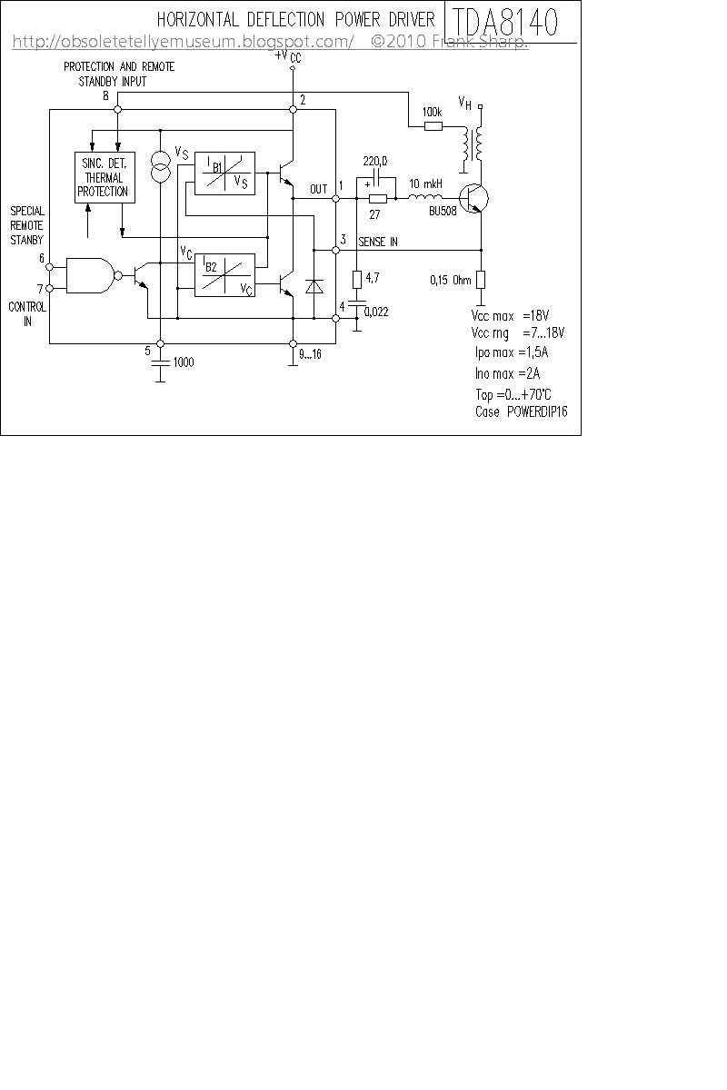 For the turn-OFF, the base of the power transistor
must be discharged by a quasi linear time decreasing
current as given in Figure 6.
Conventional driver systems inherently result into
a stable condition with a constant peak current
magnitude.
This is due to the constant base charge in the
turn-ON phase independent from the collector current
; hence a high peak current results into a low
storage time of the transistor because the excess
base charge is a minimum and vice versa. In the
active deflection the required function, high peak
current-fast switch-OFF and low peak current-slow
switch-OFF, is obtained by a controlled base discharge
current for the power transistor ; the negative
slope of this ramp is proportional to the actual
sensed current.
As a result, the active driving system even improves
the sharpnessof vertical lines on the screen
compared with the traditional solution due to the
increasedstability factor of the loop representedas
the variation of the storagetime versus the collector
peak current.
TDA8170 TV VERTICAL DEFLECTI
ON OUTPUT CIRCUITThe functions incorporated are :.POWERAMPLIFIER
.FLYBACKGENERATOR
.REFERENCE VOLTAGE
.THERMAL PROTECTION
DESCRIPTION
The TDA8170 is a monolithic integrated circuit in
HEPTAWATTTM package. It is a high efficiency
power booster for direct driving of verticalwindings
of TV yokes. It is intended for use in Colour and B
&Wtelevision receivers as well as in monitorsand
displays.


This is a semi modular chassis:
Tuner 29504.101.01 (with SIEMENS TUA2000 - 4 as mixer + OSC) + (TSA5511 - PHILIPS = Frequency synthesizer and prescaler)
(Memory SDA2216 - SIEMENS)
IF (VIF + SIF + Synchro) (VIF Video IF with TDA4442 Telefunken)
(SIF Sound IF with TBA120T Telefunken)

TBA120T (Siemens) SIF (Sound IF)
(Synch With TDA2579 PHILIPS
Luminance + Crominance (TDA3562A PHILIPS).
TDA3562A (Philips)PAL/NTSC ONE-CHIP DECODERDESCRIPTION

The TDA3562A is a monolithic IC designed as
decode PAL and/or NTSC colour television standards
and it combines all functions required for the
identification and demodulation of PAL and NTSC
signals.
.CHROMINANCE SIGNAL PROCESSOR
.LUMINANCE SIGNAL PROCESSING WITH
CLAMPING
.HORIZONTAL AND VERTICAL BLANKING
.LINEAR TRANSMISSION OF INSERTED
RGB SIGNALS
.LINEAR CONTRAST AND BRIGHTNESS
CONTROL ACTING ON INSERTED AND MATRIXED
SIGNALS
.AUTOMATIC CUT-OFF CONTROL
.NTSC HUE CONTROL
FEATURES
· A black-current stabilizer which
controls the black-currents of the
three electron-guns to a level low
enough to omit the black-level
adjustment
· Contrast control of inserted RGB
signals
· No black-level disturbance when
non-synchronized external RGB
signals are available on the inputs
· NTSC capability with hue control.
APPLICATIONS
· Teletext/broadcast antiope
· Channel number display.
GENERAL DESCRIPTION
It follows that the
external switches and filters which
are required for the TDA3562A are
not required for the TDA3566A.
There is no difference between the
amplitudes of the colour output
signals in the PAL or NTSC mode.
· The clamp capacitor at pins 10, 20
and 21 in the black-level
stabilization loop can be reduced to
100 nF provided the stability of the
loop is maintained. Loop stability
depends on complete application.
The clamp capacitors receive a
pre-bias voltage to avoid coloured
background during switch-on.
· The crystal oscillator circuit has
been changed to prevent parasitic
oscillations on the third overtone of
the crystal. Consequently the
optimum tuning capacitance must
be reduced to 10 pF.
· The hue control has been improved
(linear)
THE PHILIPS TDA3562A Circuit arrangement for the control of a pictu
re tube :1. Circuit arrangement for the control of at least one beam current in a picture tube by a picture comprising
a control loop which in one sampling interval obtains a measuring signal from the value of the beam current on the occurrence of a given reference level in the picture signal, stores a control signal derived therefrom until the next sampling interval and thereby adjusts the beam current to a value preset by a reference signal.
and a trigger circuit which suppresses auxiliary pulses used to generate the beam current after the picture tube has been started up and issues a switching signal for the purpose of closing the control loop during the sampling intervals and for releasing the control of the beam current by the picture signal after the measuring signal has exceeded the threshold value,
a change detection arrangement which delivers a change signal when the stored signal has assumed a largely constant value, and
a logic network which does not release the control of the beam current by the picture signal outside the sampling intervals until the change signal has also been issued after the switching signal.
2. Circuit arrangement as set forth in claim 1, in which the picture signal comprises several color signals for the control of a corresponding number of beam currents for the display of a color picture in the picture tube and the control loop stores a part measuring signal or a part control signal derived therefrom for each color signal,
characterized in that the change detection arrangement includes a
change detector for each color signal which delivers a part change
signal when the relevant stored signal has assumed a largely constant
value, and the logic network does not release the control of the beam
currents by the color signals outside the sampling intervals until the
part change signals have been delivered by all change detectors.
3. Circuit arrangement as set forth in claim 1, including a comparator arrangement which compares the measuring signal with the reference signal and derives the control signal from this comparison, characterized in that the change detection arrangement detects a change in the control signal with respect to time and issues the change signal when the control signal has assumed a largely constant value.
4. Circuit arrangement as set forth in claims 1, 2, 3 including a control signal memory which contains at least one capacitor, characterized in that the change detection arrangement delivers the change signal when a charge-reversing current of the capacitor occuring during the starting up of the picture tube falls below a limit value.
5. Circuit arrangement as set forth in claim 2, including a comparator arrangement which compares the measuring signal with the reference signal and derives the control signal from this comparison, characterized in that the change detection arrangement detects a change in the control signal with respect to time and issues the change signal when the control signal has assumed a largely constant value.
Description:
BACKGROUND OF THE INVENTIONThe invention relates to a circuit arrangement for the control of at least one beam current in a picture tube by a picture signal with a control loop which in one sampling interval obtains a measuring signal from the value of the beam current on the occurrence of a given reference level in the picture signal, stores a control signal derived therefrom until the next sampling interval and by this means adjusts the beam current to a value preset by a reference signal, and with a trigger circuit which suppresses auxiliary pulses used to generate the beam current after the picture tube is turned on and issues a switching signal for the purpose of closing the control loop during the sampling intervals and releasing the control of the beam current by the picture signal after the measuring signal has exceeded a threshold value.
Such a circuit arrangement has been described in Valvo Technische Information 820705 with regard to the integrated color decoder circuit PHILIPS TDA3562A and is used in this as a so-called cut-off point control. In the known circuit arrangement, such a cut-off point control provides automatic compensation of the so-called cut-off point of the picture tube, i.e. it regulates the beam current in the picture tube in such a way that for a given reference level in the picture signal the beam current has a constant value despite tolerances and changes with time (aging, thermal modifications) in the picture tube and the circuit arrangement, thereby ensuring correct picture reproduction.
Such a blocking point control is particularly advantageous for the op
eration of a picture tube
for the display of color pictures because in this case there are
several beam currents for different color components of the color
picture which have to be in a fixed ratio with one another. If this
ratio changes, for example, as the result of manufacturing tolerances or
ageing processes, distortions of the colors occur in the reproduction
of the color picture. The beam currents, therefore, have to be very
accurately balanced. The said cut-off point control prevents expensive
adjustment and maintenance time which is otherwise necessary. Conventional picutre tubes are constructed as cathode-ray tubes with hot cathodes which require a certain time after being turned on for the hot cathodes to heat up. Not until a final operating temperature has been reached do these hot cathodes emit the desired beam currents to the full extent, while gradually rising beam currents occur in the time interval when the hot cathodes are heating up. The instantaneous values of these beam currents depend on the instantaneous temperatures of the hot cathodes and on the accelerating voltages for the picture tube which build up simultaneously with the heating process and are undefined until the end of the heating time. After the picture tube is turned on, these values initially produce a highly distorted picture until the beam currents have attained their final value. These picture distortions after the picture tube is turned on are even further intensified by the fact that the cut-off point control is not yet adjusted to the beam currents which flow after the heating time is over.
For the purpose of suppressing distorted pictures during the heating time of the hot cathodes, the known circuit arrangement has a turn-on delay element operating as a trigger circuit which, in essence, contains a bistable flip-flop. When the picture tube and the circuit arrangement controlling the beam currents flowing in it are turned on, the flip-flop is switched into a first state in which it interrupts the supply of the picture signal to the picture tube. Thus, during the heating time the beam currents are suppressed, and the picture tube does not yet display any picture. In sampling intervals which are provided subsequent to flybacks of the cathode beam into an initial position on the changeover from the display of one picture to the display of a subsequent picture and even within the changeover, that is outside the display of pictures, the picture tube is controlled for a short time in such a way that beam currents occur when the hot cathodes are sufficiently heated up and an accelerating voltage is resent. If these currents exceed a certain threshold value, the flip-flop circuit switches into a second state and releases the picture signal for the control of the beam currents and the cut-off point control.
It is found, however, that the
picture
displayed in the picture tube immediately after the switching over of
the flip-flop is still not fault-free. Because, in fact, the beam
currents are supported during the heating time of the hot cathodes, the
cut-off point control cannot respond yet. This response of the cut-off
point control takes place only after the beam currents are switched on,
i.e. after the flip-flop is switched into the second state and therefore
at a time in which the picture signal already controls the beam
currents. In this way the response of the blocking point control makes
its presence felt in the picture displayed. With the known circuit arrangement the brightness of the picture gradually increases, during the response of the cut-off point control, from black to the final value.
This slow increase in the picture brightness after the tube is turned on is disturbing to the eyes of the viewer not only in the case of the black-and-white picture tubes with one hot cathode, but especially so in the case of colour picture tubes which usually have three hot cathodes. With a color picture tube, color purity errors can also occur in addition to the change in the picture brightness if, as a result of different speeds of response of the cut-off point control for the three beam currents, there are found to be intermittent variations from the interrelation between the beam currents required for a correct picture reproduction.
SUMMARY OF THE INVENTION
The aim of the invention is to create a circuit arrangement which suppresses the above-described disturbances of brightness and color of the displayed picture when the picture tube is being started.
The invention achieves this aim in that a circuit arrangement of the type mentioned in the preamble contains a change detection arrangement which emits a change signal when the stored signal has assumed an essentially constant value, and a logic network which does not release the control of the beam current by the picture signal until the change signal has also been emitted after the switching signal.
In the circuit arrangement according to the invention, therefore, the display of the picture is suppressed after the picture tube is turned on until the cut-off point control has
responded. If the picture signal then starts
to control the beam current, a perfect picture is displayed immediately.
In this way, all the disturbances of the picture which affect the
viewer's pleasure are suppressed. The circuit arrangement of the
invention is of simple design and can be combined on one semiconductor
wafer with the existing picture signal processing circuits and also, for
example, with the known circuit arrangement for cut-off point control.
Such an integrated circuit arrangement not only requires very little
space on the semiconductor wafer, but also needs no additional external
leads. Thus the circuit arrangement of the invention can be arranged,
for example, in an integrated circuit which has precisely the same
external connections as known integrated circuits. This means that an
integrated circuit containing the circuit arrangement of the invention
can be directly incorporated in existing equipment without the need for
additional measures. In one embodiment of the said circuit arrangement, in which the picture signal contains several color signals for the control of a corresponding number of beam currents for representing a color picture in the picture tube and, for each color signal, the control loop stores a part measuring signal or a part control signal derived from it, the change detection arrangement contains a change detector for each color signal which emits a part change signal when the relevant stored signal has assumed an essentially constant value, and the logic network does not release the control of the beam currents by the color signals outside the sampling intervals until the part change signals have been emitted from all change detectors.
In principle, therefore, such a circuit arrangement has three cut-off point controls for the three beam currents controlled by the individual color signals. To reduce the cost of the circuitry, the measuring stage is common to all the cut-off point controls, as in the known circuit arrangement. All three beam currents are then measured successively by this measuring stage. In this way, a part measuring signal or a part control signal derived from it is obtained for each beam current and is stored sesparately according to which of the beam currents it belongs. Changes in the part measuring signal or part control signal are detected for each beam current by one of the change detectors each time. Each of these change detectors issues a part change signal to the logic network. The latter does not release the control of the beam currents by the picture signal outside the sampling intervals until all the part change signals indicate that the part measuring signal or the part control signal, as the case may be, remains constant. This ensures that the cut-off point controls for the beam currents of all color signals have responded when the picture appears in the picture tube.
In a further embodiment of the circuit arrangement according to the invention with a comparator arrangement which compares the measuring signal with the reference signal and derives the control signal from this comparison, the change detection arrangement detects a change in the control signal with respect to time and issues the change signal when the control signal has assumed an essentially constant value. In the case of the representation of a color signal the comparator arrangement derives several part control signals, whose changes with time are detecte
d by the change detectors, from a
corresponding comparison of the part measuring signals with the
reference signal. In this embodiment of the circuit arrangement of the
invention, preference is given to storage of only the control signal or
the part control signals for the purpose of controlling the beam
currents. In another embodiment of the circuit arrangement of the invention which includes a control signal memory which contains at least one capacitor in which a charge or voltage corresponding to the control signal is stored, the change detection arrangement issues the change signal when a charge-reversing current of the capacitor occurring during the turning on of the picture tube has fallen below a limit value and has thus at least largely decayed. Such a detection of the steady state of the cut-off point control is independent of the actual magnitude of the control signal and therefore independent of, for example, the level of the picture tube cut-off voltage, circuit tolerances or ageing processes in the circuit arrangement or the picture tube.
Detection of whether or not the charge-reversing current exceeds the limit value is performed preferentially by a current detector which is designed with a current mirror system which is arranged in a supply line to a capacitor acting as a control signal store. A current mirror arrangement of this kind supplies a current which coincides very precisely with the charging current of the capacitor. This current is then compared, preferably in a further device contained in the change detection arrangement, with a current representing a limit value or, after conversion into a voltage, with a voltage representing the limit value. The change signal is obtained from the result of this comparison.
On the other hand, digital memories may also be used as control signal memories, especially when the picture signal is supplied as a digital signal and the blocking point control is constructed as a digital control loop. In such a case, the comparator arrangement, the change detection arrangement and the trigger circuit are also designed as digital circuits. Then, the change detection arrangement advantageously forms the difference of the signals stored in the control signal memory in two successive sampling intervals and compares this with the limit value formed by a digital value. If the difference falls short of the limit value, the change signal is issued.
BRIEF DESCRIPTION OF THE DRAWINGS
An embodiment of the invention is described in greater detail below with the aid of the drawings in which:
FIG. 1 shows a block circuit diagram of the embodiment,
FIG. 2 shows a somewhat more detailed block circuit diagram of the embodiment,
FIG. 3 shows time-dependency diagrams of some signals occurring in the circuit diagram shown in FIG. 2, and
FIG. 4 shows a somewhat moredetailed block circuit diagram of a part of the circuit diagram shown in FIG. 2.
 DETAILED DESCRIPTION OF THE INVENTION
FIG. 1 shows a block circuit diagram of a circuit arrangement to which a picture signal is fed via a first input 1 of a combinatorial stage 2. From the output 3 of the combinatorial stage 2 the picture signal is fed to the picture signal input of a controllable amplifier 5 which at an output 6 issues a current controlled by the picture signal. This current is fed via a measuring stage 7 to a hot cathode 8 in a picture tube 9 and forms therein a beam current of a cathode ray by means of which a picture defined by the picture signal is displayed on a fluorescent screen of the picture tube 9.
The measuring stage 7 measures the current fed to the hot cathode 8, i.e. the the beam current in the picture tube 9, and at a measuring signal output 10, issues a measuring signal corresponding to the magnitude of this current. This is fed to a measuring signal input 11 of a comparator arrangement 12 to which a reference signal is supplied at a reference signal input 13. In a preferably periodically recurring sampling interval during the occurrence of a given reference level in the picture signal, the comparator arrangement 12 forms a control signal from the value of the measuring signal fed to the measuring signal input 11 at this time, on the one hand, and the reference signal, on the other, by means of substraction and delivers this at a control signal output 14. From there the control signal is fed to an input 15 of a control signal memory 16 and is stored in the latter. The control signal is fed via
an output 17
of the control signal memory 16 to a second input 18 of combinatorial
stage 2 in which it is combined with the picture signal, e.g. added to
it. The combinatorial stage 2, the controllable amplifier 5, the measuring stage 7, the comparator arrangement 12 and the control signal memory 16 form a control loop with which the beam current is guided towards the reference signal in the sampling interval during the occurrence of the reference level in the picture signal. For the reference level, use is made in particular of a black level or a level with small, fixed distance from the black level, i.e. a value in the picture signal which produces a black or almost back picture area in the displayed picture in the picture tube. In this case the control loop, as described, forms a cut-off point control for the picture tube. If the reference level is away from the black level, the control loop is also designated as quasi-cut-off-point control.
The circuit arrangement as shown in FIG. 1 also has a trigger circuit 19 to which the measuring signal from the measuring signal output 10 of measuring stage 7 is fed at a measuring signal input 20. When the circuit arrangement and therefore the picture tube are turned on, the trigger circuit 19 is set in a first state in which by means of a first connection 21 it blocks the comparator arrangement 12 in such a way that the latter delivers no control signal or a control signal with the value zero at its control signal output 14. This prevents the control signal memory 16 from storing undefined values for the control signal at the moment of turning on or immediately thereafter.
The circuit arrangement shown in FIG. 1 also has a logic network 22 which is connected via a second connection 23, by means of which a switching signal is supplied, with the trigger circuit 10 and via a third connection 24 with the controllable amplifier 5. Like the trigger circuit 19, the logic network 22 also finds itself controlled, when the circuit arrangement is being turned on, by the switching signal in a first stage in which by way of the third connection 24 it blocks the controllable amplifier 5 with a blocking signal in such a way that no beam currents controlled by the picture signal can yet flow in the picture tube 9. Thus the picture tube 9 is blanked; no picture is displayed yet.
When picture tube 9 is turned on, the hot cathode 8 is still cold so that no beam current can flow anyhow. The hot cathode 8 is then heated up and, after a certain time, begins gradually to emit electrons as the result of which a cathode ray and therefore a beam current can form. However, during the heating up of the hot cathode 8, and because the cut-off point control has not yet responded, this would be undefined and is therefore suppressed by the controllable amplifier 5. Only in time intervals which are provided immediately subsequent to flybacks of the cathode rays into an initial position at the changeover from the display of one image to that of a subsequent image, but even before the start of the display of the subsequent image, the controllable amplifier 5 delivers a vo
ltage in the form of an auxiliary
pulse for a short time at its output 6, and when the hot cathode 8 in
the picture tube 9 is heated up sufficiently, this voltage produces a
beam current. The time interval for the delivery of this voltage is
selected in such a way that a cathode ray produced by its does not
produce a visible image in the picture tube 9, and coincides for example
with the sampling interval.The measuring stage 7 measures the short-time cathode current produced in the manner described and, at its measuring signal output 10, delivers a corresponding measuring signal which is passed via measuring signal output 20 to the trigger circuit 19. If the measuring signal exceeds a definite preset threshold value, the trigger circuit 19 is switched into a second state in which it releases the comparator arrangement 12 via the first connection 12 and, by means of the second connection 23, uses the switching signal to also bring the logic network 22 into a second state. The comparator arrangement 12 now evaluates the measuring signal supplied to it via the measuring signal input 11, i.e. it forms the control signal as the difference between the measuring signal and the reference signal supplied via the reference signal input 13. The control signal is transferred via the control signal output 14 and the input 15 into the control signal memory 16. It is subsequently fed via the output 17 of the control signal memory 16 to the second input 18 of the combinatorial stage 2 and is there combined with the picture signal at the first input 1, e.g. is superimposed on it by addition. This superimposed picture signal is fed to the picture signal input 4 of the controllable amplifier 5 via the output 3 of the combinatorial stage 2.
In the second state of the logic network 22 the
controllable amplifier 5 is
switched via the third connection 24 by the blocking signal in such a
way that the picture signal controls the beam currents only during the
sampling intervals and that, for the rest, no image appears yet in the
picture tube. The cut-off point control now gebins to respond, i.e. the
value of the control signal is changed by the control loop comprising
the combinatorial stage 2, the controllable amplifier 5, the measuring
stage 7, the comparator arrangement 12 and the control signal memory 16
until such time as the beam current in the picture tube 9 at the
blocking point or at a fixed level with respect to it is adjusted to a
value preset by the reference signal. For this purpose the sampling
interval, in which the picture signal controls the beam current via the
controllable amplifier 5 is selected in such a way that within it the
picture signal just assumes a value corresponding to the cut-off point
or to a fixed level with respect to it.During the response of the cut-off point control the control signal fed to the control signal memory 16 changes continuously. Between the control signal output 14 of the comparator arrangement 12 and the input 15 of the control signal memory 16 is inserted a changed detection arrangement 25 which detects the variations of the control signal. When the cut-off point control has responded, i.e. the control signal has assumed a constant value, the change detection arrangement 25 delivers a change signal at an output 26 which indicates that the steady stage of the cut-off
point control is
achieved and the said signal is fed to a change signal input 27 of the
logic network 22. The logic network then switches into a third state in
which via the third connection 24 it enables the controllable amplifier 5
in such a way that the beam currents are now controlled without
restriction by the picture signal. Thus a correctly represented picture
appears in the picture tube 9. A shadow-like representation of individual constituents of the circuit arrangement in FIG. 1 is used to indicate a modification by which this circuit arrangement is equipped for the representation of color pictures in the picture tube 9. For example, three color signals are fed in this case as the picture signal via the input 1 to the combinatorial stage 2. Accordingly, the input 1 is shown in triplicate, and the combinatorial stage 2 has a logic element, e.g. an adder, for example of these color signals. The controllable amplifier 5 now has three amplifier stages, one for each of the color signals, and the picture tube now contains three hot cathodes 8 instead of one so that three independent cathode rays are available for the three color signals.
However, to simplify the circuit
arrangement and to save on components, only one measuring stage 7 is
provided which measures all three beam currents successively. Also, the
comparator arrangement 12 forms part control signals from the
successively arriving part measuring signals for the individual beam
currents with the reference signal, and these part control signals are
allocated to the individual color signals and passed on to three storage
units which are contained in the control signal memory 16. From there,
the part control signals are sent via the second input 18 of the
combinatorial stage 2 to the assigned logic elements. The circuit arrangement thus forms three independently acting control loops for the cut-off point control of the individual color signals, in which case only the measuring stage 7 and to some extent at least the comparator arrangement 12 are common to these control loops.
The change detection arrangement 25 now has three change detectors each of which detects the changes with time of the part control signals relating to a color signal. Then via the output 26 each of these change detectors delivers a part change signal to the change signal input 27 of the logic network 22. These part change signals occur independently of one another when the relevent control loop has responded. The logic network 22 evaluates all three part change signals and does not switch into its third stage until all part change signals indicate a steady state of the control loops. Only then, in fact, is it ensured that all the color signals from the beam currents controlled by them are correctly reproduced in the picture tube, and thus no distortions of the displayed image, especially no color purity errors, occur. The color picture displayed then immediately has the correct brightness and color on its appearance when the picture tube is turned on.

FIG. 2 shows a somewhat more detailed block circuit diagram of an embodiment of a circuit arrangement equipped for the processing of a picture signal containing three colour signals. Three color signals for the representation of the colors red, green and blue are fed to this circuit arrangement via three input terminals 101, 102, 103. A red color signal is fed via the first input terminal 101 to a first adder 201, a green colour signal is fed via the second input terminal to a second adder 202, and a blue colour signal is fed via the third input terminal 103 to a third adder 203. From outputs 301, 302 and 303 of the adders 201, 202, 203 the color signals are fed to amplifier stages 501, 502 and 503 respectively. Each of the amplifier stages contains a switchable amplifier 511, 512 and 513, an output amplifier 521, 522 and 523 as well as a measuring transistor 531, 532 and 533 respectively. The emitters of these measuring transistors 531, 532, 533 are each connected to a hot cathode 801, 802, 803 of the picture tube 9 and deliver the cathode currents, whereas the collectors of measuring transistors 521, 532, 533 are connected to one another and to a first terminal 701 of a measuring resistor 702 the second terminal of which 7
03 is connected to earth. The
current gain of the measuring transistors 531, 532 and 533 is so great
that their collector currents coincide almost with the cathode currents.
By measuring the voltage drop produced by the cathode currents at the
measuring resistor 802 it is then possible to measure the cathode
currents and therefore the beam currents in the picture tube 9 with
great accuracy. The falling voltage at the measuring resistor 702 is fed as a measuring signal to an input 121 of a buffer amplifier 120 with a gain factor of one, at the output 122 of which the unchanged measuring signal is therefore available at low impedance. From there it is fed to a first terminal 131 of a reference voltage source 130 which is connected with its second terminal 132 to inverting inputs 111, 112 and 113 of three differential amplifiers 123, 124, 125 respectively. The differential amplifiers 123, 124, 125 also each have a non-inverting input 114, 115, and 116 respectively. These are connected to each other at a junction 117, to earth via a leakage current storage capacitor 126 and to the output 122 of the buffer amplifier 120 via decoupling resistor 118 and a leakage current sampling switch 119. In addition, the input 121 of the buffer amplifier 120 can be connected to earth via a short-circuiting switch 127.

The operation of the comparator arrangement 12 which consists mainly of the buffer amplifier 120, the reference voltage source 130 and differential amplifiers 123, 124, 125 will be explained below with the aid of the pulse diagrams in FIG. 3. FIG. 3a shows a horizontal blanking signal for a television signal which, as the picture signal, controls the beam currents in the picture tube 9. In this diagram, H represents horizontal blanking pulses which follow one another in the picture signal at the time interval of one line duration and by means of which the beam currents are switched off during line flyback between the display of the individual picture lines in the picture tube. FIG. 3b shows a vertical blanking pulse V by means of which the beam currents are switched off during the change ober from the display of one picture to the display of the next picture. FIG. 3c shows a measuring signal control pulse VH which is formed from a vertical blanking pulse lengthened by three line duration.
The short-circuiting switch 127 is now controlled in such a way that it is non-conducting only throughout the duration of the measuring signal control pulse VH and during the remaining time short-circuits the input 121 of the buffer amplifier 120 to earth. This means that a measuring signal only reaches the comparator arrangement 12 during frame change so that the parts of the picture signal which control the beam currents producing the picture in the picture tube exert no influence on comparator arrangement 12 and therefore on the blocking point control.
Throughout the duration of the measuring signal control pulse VH, the measuring signal from output 122, reduced by a reference voltage issued by the reference voltage source 130 between its first 131 and its second terminal 132, is present at the inverting inputs 111, 112, 113 of differential amplifiers 123, 124, 125. If the differential amplifiers 123, 124, 125 were not present, this difference would be fed directly as part control signals to the control signal storage capacitors 161, 162, 162. The differential amplifiers 123, 124, 125 amplify the difference and thus for
m the control amplifiers of the control loops. The comparator arrangement 12 further contains a device for compensation of the influence of any leakage currents occurring in the picture tube 9. For this purpose, a voltage to which the leakage current storage capacitor 126 is charged is fed to the non-inverting inputs 114, 115, 116 of the three differential amplifiers 123, 124 and 125. The charging is performed by the measuring signal from output 122 of the buffer amplifier 120 via the decoupling resistor 118 and the leakage current sampling switch 119 which is closed only within the period of the vertical blanking pulse V, and in certain cases only during part of the latter. Within this time the beam currents are, in fact, totally switched off by the picture signal so that in certain cases only a leakage current flows through the measuring resistor 702. Consequently, throughout the duration of the vertical blanking pulse V the measuring signal corresponds to this leakage current. Because the leakage current also flows during the remaining time, even outside the duration of the vertical blanking pulse the measuring signal contains a component originating from the leakage current which therefore is also contained in the voltage fed to the inverting inputs 111, 112, 113 of differential amplifiers 123, 124, 125 and is subtracted out in the differential amplifiers 123, 124, 125.
The part control signal is fed from output 141 of differential amplifier 123 by the first control signal sampling switch 154 to the first terminal 151 of the first control signal storage capacitor 161 during the period of a storage pulse L1 and is stored in the said capacitor. Similarly, the part control signal from output 143 of differential amplifier 125 is fed to the third control signal storage capacitor 163 during the period of a storage pulse L2 and the part control signal from output 142 of differential amplifier 124 is fed to the second control signal storage capacitor 162 during a storage pulse L3. The storage pulses L1, L2 and L3 are illustrated in FIGS. 3d, e and f. They lie in sequence in one of the three line periods by which the measuring signal control pulse VH is longer than the vertical blan
king pulse V. These three line periods form
the sampling interval for the measuring signal or the part measuring
signals, as the case may be. During the remaining periods the outputs,
141, 152, 143 of the differential amplifiers 123, 124, 125 are isolated
from the control signal storage capacitors 161, 162, 163 so that no
interference can be transmitted from there and any distortion of the
stored part control signals caused thereby is eliminated. For the
duration of storage pulses L1, L2 and L3 the color signals at the input
terminals 101, 102, 103 are at their reference level i.e. in the present
embodiment at a level, corresponding to the blocking point or at a
fixed level with respect to it so that the control loops can adjust to
this level.The switchable amplifiers 511, 512, and 513 each receive at each input 241, 242, 243 a blanking signal BL1, BL2, BL3 respectively, the curves of which are shown in FIGS. 3g, h, i. These blanking signals interrupt the supply of the color signals during line flybacks and frame change, i.e. during the period of the measuring signal control pulse VH, and thus the beam currents in these time intervals are switched off. Naturally, the red color signal is let through during the first line period after the end of the vertical blanking pulse V, the blue color signal during the second line period after the end of the vertical blanking pulse V and the green color signal during the third line period after the end of the vertical blanking pulse V by the switchable amplifiers 511, 512, 513 respectively so that they can control the beam currents. Blanking signals BL1, BL2 and BL3 also provide for interruptions in the frame change blanking pulse, which corresponds to the measuring signal control pulse, in the corresponding time intervals. In these time intervals the beam currents are measured and part control signals are determined from the part measuring signals and stored in the control signal storage capacitors 161, 162, 163.
The circuit arrangement shown in FIG. 2 further contains a trigger circuit 19 to which a supply voltage is fed via a supply terminal 190. Via a reset input 191 a voltage is also
supplied to
the trigger circuit 19 from a third terminal 133 of the reference
voltage source 130. When the circuit arrangement is turned on, this
voltage is designed so as to be delayed with respect to the supply
voltage so that when the circuit arrangement is brought into operation
the interplay of the two voltages produces a switch-on reset signal such
that a low-value voltage pulse occurs at the reset input 191 during
turn on, which means that the trigger circuit 19 is set in its first
state. The reset input 191 can also be connected to another circuit of
any configuration which generates a switch-on reset signal when the
picture tube is turned on. The trigger circuit 19 is further connected via a second connection 23 to a logic network 22 which, when the circuit arrangement is turned on, is also set into a first state via the second connection 23. In this first state the logic network 22 delivers a blocking signal at a blocking output 240 which is fed to the three switchable amplifiers 511, 512, 513. By this means the supply of the color signals to the output amplifiers 521, 522, 523 is interrupted completely so that no beam currents can be generated by these. No picture is therefore displayed.
An insertion signal EL which extends over the three line periods by which the measuring signal control pulse VH is longer than the vertical blanking pulse V, i.e. over the sampling interval, is also fed via a line 233 to the trigger circuit 19 and the logic network 22. As long as the trigger circuit 19 is in its first state, this insertion pulse EL is issued via a control output 192 from the trigger circuit 19 and fed to the pulse generator 244. During the period of the insertion pulse EL this generator produces a voltage pulse of a definite magnitude and passes this to output amplfiiers 521, 522, 523 as an auxiliary pulse via switching diodes 245, 246, 247. By this means the beam currents are s
witched on for a short
time so as to receive a measuring signal despite the disconnected color
signals as soon as at least one of the hot cathodes 801, 802, 803
delivers a beam current. In its first state the trigger circuit 19 also delivers a signal via a control line 211, and this signal is used to switch the outputs 141, 142, 143 of the differential amplifiers 123, 124, 125 to earth potential or practically to earth potential. This suppresses effects of voltages at the inputs 111 to 116 of the differential amplifiers 123, 124, 125, especially effects of the reference voltage source 130 which may in some cases initiate incorrect charging of the control signal storage capacitors 161, 162, 163.
The measuring signal produced by means of the pulse generator 244 at the input 121 of the buffer amplifier 120 is also fed to the trigger circuit 19 via a measuring signal input 20. If it exceeds a preset threshold value, the trigger circuit 19 switched into its second state. The logic network 22 is then also switched into its second state via the second connection 23. The differential amplifiers 123, 124, 125, too, are triggered by the signal along the control line 211 into issuing a control signal defined by the difference in the voltages at its inputs 111 to 116. The pulse generator 244 is blocked by the control output 192. The blocking signal issued from the blocking output 240 of the logic network 22 now turns on the switchable amplifiers 511, 512, 513 in the time intervals defined by the storage pulses L1, L2, L3 in such a way that in these time intervals the color signals can produce beam currents to form a measuring signal by which the control loops respond. However, the display of the picture is still suppressed. The control signal storage capacitors 161, 162, 163 are charged up in this process. In the leads to the first terminals 151, 152, 153 there are change detectors 251, 252, 253 which detect the changes of the charging currents of the control signal storage capacitors 161, 162, 163 and at their outputs 261, 262, 263 in each case deliver a part change signal when the charging current of the control signal storage capacitor in question has decayed and thus the relevant control loop has responded. The part change signals are fed to three terminals 271, 272, 273 of the change signal input 27 of the logic network 22.
When part change signals are present from all change detectors 251, 252, 253, when therefore all control loops have responded, the logic network 22 switches from its second to its third state. The blocking signal from the blocking output 240 is now completely disconnected such that the switchable amplifiers 511, 512, 513 are now switched only by the blanking signals BL1, BL2, BL3. The colour signals are then switched through to the output amplifiers 521, 522, 523 and the picture is displayed in the picture tube.

FIG. 4 shows an embodiment for a trigger circuit 19 and a logic network 22 of the circuit arrangements as shown in FIGS. 1 or 2. The trigger circuit 19 contains a flip-flop circuit formed from two NAND-gates 194, 195 to which the switch-on reset signal, by which the trigger circuit 19 is returned to its first stage, is fed via the reset input 191. All the elements of the circuit arrangement in FIG. 4 are shown in positive logic. Thus, a short-time low voltage at the reset input 191 immediately after the circuit arrangement is started up is used to set the flip-flop circuit 194, 195 in such a way that a high voltage occurs at the output of the second NAND gate 194 and a low voltage at the output of the second NAND gate 195. The low voltage at the output of the second NAND gate 195 blocks differential amplifiers 123, 124, 125 via the control line 211 in the manner described.
The insertion pulse EL is fed via the line 233 to the trigger circuit 19, is combined via an AND gate 196 with the signal from the output of the first NAND gate 194 and is delivered at the control output 192 for the purpose of controlling the pulse generator 244.
The signals from the outputs of the NAND-gates 194, 195 are fed via a first line 231 and a second line 232 of the second connection 23 as a switching signal to the logic network 22. The first line 231 is connected to reset inputs R of three part change signal memories 221, 222, 223 in the form of bistable flip-flop circuits which when the circuit arrangement is started up are reset via the first line 231 in such a way that they carry a low voltage at their outputs Q. The second line 232 of the second connection 23 leads via three AND gates 224, 225, 226 to setting inputs S of the three part change signal memories 221, 222, 223. By means of the AND gates 224, 225, 226 the signal on the second line 232 of the second connection 23 is combined each time with on
e of the part change signals supplied via
the terminals 271, 272, 273. The signals from the outputs Q of the part
change signal memories 221, 222, 223 are combined by means of a
collecting gate 227 in the form of an NAND gate and are held ready at
its output 228. The measuring signal is fed to the trigger circuit 19 via the measuring signal input 20 and passed to a first input 197 of a threshold detector 198 to which at a second input a threshold value, in the form of a threshold voltage for example, produced by a threshold generator 199 is also supplied. When the voltage at the first input 197 of the threshold detector 198 is smaller than the voltage delivered by the threshold generator 199, the threshold detector 198 delivers a high voltage at its output 200. When, on the other hand, the voltage at the first input 197 is greater than the voltage of the threshold generator 199, the voltage at the output 200 jumps to a low value. This voltage is supplied as the setting signal of the flip-flop circuit 194, 195, reverses the latter and thereby switches the trigger circuit 19 into its second state when the voltage at the first input 197 exceeds the voltage of the threshold generator 199.
Between the output 200 and the flip-flop circuit 194, 195 in the circuit arrangem
ent
shown in FIG. 4 there is inserted an inquiry gate 181 in the form of an
OR gate to which an inquiry pulse is fed via an inquiry input 193 of
the trigger circuit 19. This ensures that the flip-flop circuit 194, 195
is switched over only at a time fixed by the inquiry pulse--in the
present case a negative voltage pulse--and not at any other times due to
disturbances. As such an inquiry pulse it is possible to use, for
example, a pulse which occurs in the second line period after the end of
the vertical blanking pulse V, i.e. one which largely corresponds to
the storage pulse L2. After the switching over of the flip-flop circuit 194, 195 corresponding to the setting of the trigger circuit 19 into the second state, appropriately modified signals are supplied via the control line 211 and the output 192 for the purpose of controlling the pulse generator 244 and the differential amplifiers 123, 124, 125. Modified voltages also appear on the lines 231, 232 of the second connection
23, and these voltages release the part change signal
memories 221, 222, 223 such that they can each be set when the part
change signals reach the terminals 271, 272, 273. In certain cases, a further flip-flop circuit 234 is inserted in the lines 231, 232 to delay the signals passing along these lines; this is reset via the first line 231 when the circuit arrangement is started up and thus it also resets the part change signal memories 221, 222, 223. However, after the trigger circuit 19 is switched into the second state the further flip-flop circuit 234 is not set via the second line 232 of the second connection 23 until a release pulse arrives via a release input 235 and another AND gate 236, for example a period of approximately the interval of two vertical blanking pulses V after the switching of the trigger circuit 19 into the second state. In this way it is possible to bridge a period of time in which no defined signal values are present at the terminals 271, 272, 273.
The signal at the output 228 of the collecting gate 227 changes its state when the last of the three part change signals has also arrived and has set the last of the three part change signal memories. The signal is then combined via a gate arrangement 229 of two NAND gates and one AND gate with the insertion pulse EL of line 223 and with the signal on the second line 232 of the second connection 23 or from the output Q of the further flip-flop circuit 234 to the blocking signal delivered at the blocking output 24 which is fed to the switchable amplifiers 511, 512, 513.
The circuit arrangement described is designed in such a way that the trigger circuit 19 remains in its second state and logic network 22 remains in its third state even if charging currents reappear at the difference signal storage cpacitors 161, 162, 163 due to disturbances during the operation of the circuit arrangement. The cutoff point control then makes readjustments without the displayed picture being disturbed.
In the circuit arrangement shown in F
IG. 2, the green
color signal can also be let through during the second line period after
the end of the vertical blanking pulse V and the blue color signal
during the third line period after the end of the vertical blanking
pulse V by the switchable amplifiers 511, 512, 513 for the purpose of
controlling the beam currents. The storage pulses L2 and L3 at the
control signal sampling switches 155 and 156 and the second and third
blanking signals BL2 and BL3 at the blanking inputs 242 and 243 are then
to be interchanged. The resulting insertion signals A2 and A3 as shown
in FIGS. 3m and n are also interchanged then accordingly. In FIG. 2 a dashed line is used to indicate which components of the circuit arrangement can be combined advantageously to form an integrated circuit. The first terminals 151, 152, 153 of the difference signal storage capacitors 161, 162, 163, one terminal 128 of leakage current storage capacitor 126, three terminals 524, 525, 526 in the leads to the output amplifiers 521, 522, 523 as well as a line connection 704 between the first terminal 701 of the measuring resistor 702 and the input 121 of the buffer amplifier 120 will then form the connecting contacts of this integrated circuit
PHILIPS TDA2579 Horizontal/vertical synchronization circuit GENERAL DESCRIPTION
The TDA2579B generates and synchronizes horizontal and vertical signals. The device has a 3 level sandcastle output;
a transmitter identification signal and also 5
0/60 Hz identification.Features
· Horizontal phase detector, (sync to oscillator), sync separator and noise inverter
· Triple current source in the phase detector with automatic selection
· Second phase detector for storage compensation of the horizontal output
· Stabilized direct starting of the horizontal oscillator and output stage from mains supply
· Horizontal output pulse with constant duty cycle value of 29 ms
· Internal vertical sync separator, and two integration selection times
· Divider system with three different reset enable windows
· Synchronization is set to 628 divider ratio when no vertical sync pulses and no video transmitter is identified
· Vertical comparator with a low DC feedback signal
· 50/60 Hz identification output combined with mute function
· Automatic amplitude adjustment for 50 and 60 Hz and blanking pulse duration
· Automatic adaption of the burst-key pulsewidth.
FUNCTIONAL DESCRIPTION
Vertical part (pins 1,2,3,4)
The IC embodies a synchronized divider system for generating the vertical sawtooth at pin 3. The divider system has an
internal frequency doubling circuit, so the horizontal oscillator is working at its normal line frequency and one line period
equals 2 clock pulses. Due to the divider system no vertical frequency adjustment is needed. The divider has a
discriminator window for automatically switching over from the 60 Hz to 50 Hz system. The divider system operates with
3 different divider reset windows for maximum interference/disturbance protection.
The windows are activated via a
n up/down counter. The counter increases its counter value by 1 for each time theseparated vertical sync pulse is within the searched window. The count is decreased by 1 when the vertical sync pulse
is not present.
Large (search) window: divider ratio between 488 and 722
This mode is valid for the following conditions:
1. Divider is looking for a new transmitter.
2. Divider ratio found, not within the narrow window limits.
3. Up/down counter value of the divider system operating in the narrow window mode decreases below count 1.
4. Externally setting. This can be reached by loading pin 18 with a resistor of 220 kW to earth or connecting a 3.6 V
diode stabistor between pin 18 and ground.
Narrow window: divider ratio between 522-528 (60 Hz) or 622-628 (50 Hz).
The divider system switches over to this mode when the up/down counter has reached its maximum value of 12 approved
vertical sync pulses. When the divider operates in this mode and a vertical sync pulse is missing within the window the
divider is reset at the end of the window and the counter value is decreased by 1. At a counter value below count 1 the
divider system switches over to the large window mode.
Standard TV-norm
When the up/down counter has reached its maximum value of 12 in the narrow window mode, the information applied to
the up/down counter is changed such that the standard divider ratio value is tested. When the counter has reache
d avalue of 14 the divider system is changed over to the standard divider ratio mode. In this mode the divider is always reset
at the standard value even if the vertical sync pulse is missing. A missed vertical sync pulse decreases the counter value
by 1. When the counter reaches the value of 10 the divider system is switched over to the large window mode.
The standard TV-norm condition gives maximum protection for video recorders playing tapes with anti-copy guards.
No-TV-transmitter found: (pin 18 <>
In this condition, only noise is present, the divider is rest to count 628. In this way a stable picture display at normal height
is achieved.
Video tape recorders in feature mode
It should be noted that some VTRs operating in the feature modes, such as picture search, generate such distorted
pictures that the no-TV-transmitter detection circuit can be activated as pin V18 drops below 1.2 V. This would imply a
rolling picture (see Phase detector, sub paragraph d). In general VTR-machines use a re-inserted vertical sync pulse in
the feature mode. Therefore the divider system has been made such that the automatic reset of the divider at count 628
when V18 is below 1.2 V is inhibited when a vertical sync pulse is detected.
The divider system also generates the anti-top-flutter pulse which inhibits the Phase 1 detector during the vertical sync.
pulse. The width of this pulse depends on the divider mode. For the divider mode a the start is generated at the reset of
the divider. In mode b and c the anti-top-flutter pulse starts at the beginning of the first equalizing pulse.
The anti-top-flutter pulse ends at count 8 for 50 Hz and count 10 for 60 Hz. The vertical blanking pulse is also generated
via the divider system. The start is at the reset of the divider while the pulse ends at count 34 (17 lines) for 60 Hz, and at
count 44 (22 lines) for 50 Hz systems. The vertical blanking pulse generated at the sandcastle output pin 17 is made b
yadding the anti-top-flutter pulse and the blanking pulse. In this way the vertical blanking pulse starts at the beginning of
the first equalizing pulse when the divider operates in the b or c mode. For generating a vertical linear sawtooth voltage
a capacitor should be connected to pin 3. The recommended value is 150 nF to 330 nF (see Fig.1).
The capacitor is charged via an internal current source starting at the reset of the divider system. The voltage on the
capacitor is monitored by a comparator which is activated also at reset. When the capacitor has reached a voltage value
of 5.85 V for the 50 Hz system or 4.85 V for the 60 Hz system the voltage is kept constant until the charging period ends.
The charge period width is 26 clock pulses. At clock pulse 26 the comparator is switched off and the capacitor is
discharged by an npn transistor current source, the value of which can be set by an external resistor between pin 4 and
ground (pin 9). Pin 4 is connected to a pnp transistor current source which determines the current of the npn current
source at pin 3. The pnp current source on pin 4 is connected to an internal zener diode reference voltage which has a
typical voltage of » 7.5 volts. The recommende
d operating current range is 10 to 75 mA. The resistance at pin R4 shouldbe 100 to 770 kW. By using a double current mirror concept the vertical sawtooth pre-correction can be set on the desired
value by means of external components between pin 4 and pin 3, or by connecting the pin 4 resistor to the vertical current
measuring resistor of the vertical output stage. The vertical amplitude is set by the current of pin 4. The vertical feedback
voltage of the output stage has to be applied to pin 2. For the normal amplitude adjustment the values are DC = 1 V and
AC = 0.8 V. Due to the automatic system adaption both values are valid for 50 Hz and 60 Hz.
The low DC voltage value improves the picture bounce behaviour as less parabola compensation is necessary. Even a
fully DC coupled feedback circuit is possible.
Vertical guard
The IC also contains a vertical guard circuit. This circuit monitors the vertical feedback signal on pin 2. When the level
on pin 2 is below 0.35 V or higher than 1.85 V the guard circuit inserts a continuous level of 2.5 V in the sandcastle output
signal of pin 17. This results in the blanking of the picture displayed, thus preventing a burnt-in horizontal line. The guard
levels specified refer to the zener diode reference voltage source level.
Driver output
The driver output is at pin 1, it can deliver a drive current of 1.5 mA at 5 V output. The internal impedance is approximately
170 W. The output pin is also connected to an internal current source with a sink current of 0.25 mA.
Sync separator, phase detector and TV-station identification (pins 5,6,7,8 and 18)
The video input signal is connected to pin 5. The sync separator is designed such that the slicing level is independent of
the amplitude of the sync pulse. The black level is measured and stored in the capacitor at pin 7. The slicing level value
is stored in the capacitor at pin 6. The slicing level value can be chosen by the value of the external resistor between
pins 6 and 7.
Black level detector
A gating signal is used for the black level detector. This signal is composed of an internal horizontal reference pulse with
a duty factor of 50% and the flyback pulse at pin 12. In this way the TV-transmitter identification operates also for all DC
conditions at input pin 5 (no video modulation, plain carrier only).
During the frame interval the slicing level detector is inhibited by a signal which starts with the anti-top flutter pulse and
ends with the reset vertical divider circuit. In this way shift of the slicing level due to the vertical sync signal is reduced
and separation of the vertical sync pulse is improved.
Noise level detector
An internal noise inverter is activated when the video level at pin 5 decreases below 0.7 V. The IC also embodies a
built-in sync puls
e noise level detection circuit. This circuit is directly connected to pin 5 and measures the noise level atthe middle of the horizontal sync pulse. When a signal-to-noise level of 19 dB is detected a counter circuit is activated.
A video input signal is processed as “acceptable noise free” when 12 out of 15 sync pulses have a noise level below
19 dB for two successive frame periods. The sync pulses are processed during a 15 line width gating period generated
by the divider system. The measuring circuit has a built-in noise level hysteresis of approximately 3 dB. When the
“acceptable noise free” condition is found the phase detector of pin 8 is switched to not gated and normal time constant.
When a higher sync pulse noise level is found the phase detector is switched over to slow time constant and gated sync
pulse phase detection. At the same time the integration time of the vertical sync pulse separator is adapted.
TDA4442 VIDEO IF AMPLIFIER:DESCRIPTION
The TDA4442 is a Video IF amplifier with standard
switch for colour or monochromeTV
sets, and VTR’s.
GENERAL DESCRIPTION
This video IF processing circuit integrates the following
functional blocks : .Three symmetrical, very stable, gain controlled
wideband amplifier stages - without feedback
by a quasi-galvanic coupling. .Demodulator controlled by the picture carrier .Video output amplifier with high supply voltage
rejection .Polarity switch for the video output signal .AGC on peak white level .GatedAGC .Discharge control .Delayed tuner AGC .At VTR Reading mode the video output signal
is at ultra white level.TSA5511 1.3 GHz Bidirectional I2C-bus controlled synthesizer
GENERAL DESCRIPTION
The
TSA5511 is a single chip PLL frequency synthesizerdesigned for TV tuning systems. Control data is entered
via the I2C-bus; five serial bytes are required to address
the device, select the oscillator frequency, programme the
eight output ports and set the charge-pump current. Four
of these ports can also be used as input ports (three
general purpose I/O ports, one ADC). Digital information
concerning those ports can be read out of the TSA5511 on
the SDA line (one status byte) during a READ operation.
A flag is set when the loop is “in-lock” and is read during a
READ operation. The device has one fixed I2C-bus
address and 3 programmable addresses, programmed by
applying a specific voltage on Port 3. The phase
comparator operates at 7.8125 kHz when a 4 MHz crystal
is used.
FEATURES
· Complete 1.3 GHz single chip system
· Low power 5 V, 35 mA
· I2C-bus programming
· In-lock flag
· Varicap drive disable
· Low radiation
· Address selection for Picture-In-Picture (PIP), DBS
tuner (3 addresses)
· Analog-to-digital converter
· 8 bus controlled ports (5 for TSA5511T), 4 current
limited outputs (1 for TSA5511T), 4 open collector
outputs (bi-directional)
· Power-down flag
APPLICATIONS
· TV tuners
· VCR Tuners.
LIST OF COMMON FAULTS / TROUBLESHOOTING GRUNDIG CHASSIS CUC3400:
Grundig CUC3400 +B decreasing when average brightness of picture increases. Change C611 47uF cap.
Grundig CUC3400 +B decreasing when average brightness of picture increases. Change C611 47uF cap.
Grundig CUC3400 Arcing/random chan change tripler
Grundig CUC3400 Blue raster with fb lines TDA3505 vid proc chip IC9531 on chroma board
Grundig CUC3400 Blue raster with flyback lines. TDA3505 video processor chip IC9531
Grundig CUC3400 dead on/off sw u/s CHS - G102
Grundig CUC3400 Dead - & tripping. Set HT control ( R637 ) int o/c , D666/D664 s/c , IC686 78M05
Grundig CUC3400 Dead - all fuses intact D691 BYV28/100 s/c (20v supply)
Grundig CUC3400 DEAD 800mA FUSE BLOWN DRY JOINTS ON CHOPPER TX CHECK D663 664 666 C653 4n7 C667 2u2
Grundig CUC3400 Dead or tripping Set HT pot R637, D666 BYV16 s/c, D664 BA159 s/c or IC686 78M05 s/c
Grundig CUC3400 Dead with buzz from Ipsalo Tfmr The +M supply ok at 11v in st/by but dropped instead of increasing to 20v when sw on. C630 0µ68 leaky
Grundig CUC3400 Dead, 800mA SI642 fuse o/c, chopper T661 BUT11A s/c Check for dry joints Ipsalo tfmr or D663, 664 & 666 faulty also check C667 2µ2
Grundig CUC3400 Dead. Drys on main PCB.
Grundig CUC3400 Int colour & rh side of pic blanked TDA2579 timebase chip
Grundig CUC3400 Int dead Pin 0 on lopt (eht overwind) arcing internally - new lopt reqd
Grundig CUC3400 Int or perm tripping - ok on dummy load Timing cap C653 4n7
Grundig CUC3400 No chan change when cold - display changes ok tho' Dry joint pin 15 tuner/if socket
Grundig CUC3400 No sound C266 1000µ 25v s/c; R367 8R2 safety res o/c
Grundig CUC3400 No start up - ticks C653 4n7 connected to pin 15 of power chip u/s
Grundig CUC3400 No start up with ticking HT at chopper coll - C653 4n7 connected to pin 15 power chip u/s
Grundig CUC3400 Poor purity & focus. C433 ( 1 , 000uf , 25v )
Grundig CUC3400 Poor R/C response R1212 33R missing in sensor pcb
Grundig CUC3400 Startup - No s/up - ticking from transformer. C653 ( 4.7nf ) connected to pin 15 of IC.
Grundig CUC3400 tripping set ht pot R637
Grundig CUC3400 Tripping comes on if adj line frequency down. C653 ( 4.7u f ).
No comments:
Post a Comment
The most important thing to remember about the Comment Rules is this:
The determination of whether any comment is in compliance is at the sole discretion of this blog’s owner.
Comments on this blog may be blocked or deleted at any time.
Fair people are getting fair reply. Spam and useless crap and filthy comments / scrapers / observations goes all directly to My Private HELL without even appearing in public !!!
The fact that a comment is permitted in no way constitutes an endorsement of any view expressed, fact alleged, or link provided in that comment by the administrator of this site.
This means that there may be a delay between the submission and the eventual appearance of your comment.
Requiring blog comments to obey well-defined rules does not infringe on the free speech of commenters.
Resisting the tide of post-modernity may be difficult, but I will attempt it anyway.
Your choice.........Live or DIE.
That indeed is where your liberty lies.
Note: Only a member of this blog may post a comment.