


HOW THYRISTOR LINE DEFLECTION OUTPUT SCAN STAGES WORK:
INTRODUCTION:
The massive demand for colour television receivers in Europe/Germany
in the 70's brought about an influx of sets from the continent. Many of
these use the thin -neck (29mm) type of 110° shadowmask tube and the
Philips 20AX CRT Tube, plus the already Delta Gun CRT .

Scanning
of these tubes is accomplished by means of a toroidally wound
deflection yoke (conventional 90° and thick -neck 110° tubes operate
with
saddle -wound deflection coils). The inductance of a toroidal yoke is
very much less than that of a saddle -wound yoke, thus higher scan currents are required.
The deflection current necessary for the line scan is about 12A peak
-to -peak. This could be provided by a transistor line output stage but a
current step-up transformer, which is bulky and both difficult and
costly to manufacture, would be required.
An entirely different
approach, pioneered by RCA in America and developed by them and by ITT
(SEL) in Germany, is the thyristor line output stage. In this system the
scanning current is provided via two thyristors and two switching diodes
which due to their characteristics can supply the deflection yoke
without a step-up transformer (a small transformer is still required to
obtain the input voltage pulse for the e.h.t. tripler). The purpose of
this article is to explain the basic operation of such circuits. The
thyristor line output circuit offers high reliability since all
switching occurs at zero current level. C.R.T. flashovers, which can
produce high current surges (up to 60A), have no detrimental effects on
the switching diodes or thyristors since the forward voltage drop across
these devices is small and the duration of the current pulses short. If
a surge limiting resistor is pro- vided in the tube's final anode
circuit the peak voltages produced by flashovers seldom exceed the
normal repetitive circuit voltages by more than 50-100V. This is well
within the device ratings. Brief Basics: LINE Scan output stages operate on the same basic principle whether
the active device used is a valve, transistor or thyristor. As a
starting point, let's remind ourselves of this principle, which was
first developed by Blumlein in 1932. The idea in its simplest form is
shown in Fig. 1. The scan coils, together with a parallel tuning
capacitor, are connected in series with a switch across the h.t. supply.
When the switch is closed - (a) - current flows through the coils,
building up linearly as required to deflect the beam from the centre to
the right-hand side of the screen. At this point the switch is opened.
The coils and the capacitor then form a resonant circuit. The magnetic
fields generated around the coils during the preceeding forward scan as
current flowed through them when the switch was closed now collapse,
charging the capacitor - (b). As a result of the resonant action the
capacitor next discharges, driving current through the coils in the
opposite direction - (c). Once more magnetic fields are generated around
the coils. This resonant action lasts for one half -cycle of
oscillation, during which the beam is rapidly deflected from the right-
hand side to the centre and then to the left-hand side of the screen.
The flyback is thus complete. If the switch is now closed again further
oscillation is prevented and, as the magnetic fields around the coils
collapse, a decaying current flows through them in the direction shown
at (d). This decaying current flow deflects the beam from the left-hand
side of the screen back towards the centre: the period during which this
occurs is often referred to as the energy recovery part of the scanning
cycle. When the current has decayed to zero we are back at the
situation shown at (a): the current through the coils reverses, driving
the beam to the right-hand side of the screen. This is a very efficient
System, since most of the energy drawn from the supply is subsequently
returned to it. There is negligible resistance in the circuit, so there
is very little power loss.
Brief Basics: LINE Scan output stages operate on the same basic principle whether
the active device used is a valve, transistor or thyristor. As a
starting point, let's remind ourselves of this principle, which was
first developed by Blumlein in 1932. The idea in its simplest form is
shown in Fig. 1. The scan coils, together with a parallel tuning
capacitor, are connected in series with a switch across the h.t. supply.
When the switch is closed - (a) - current flows through the coils,
building up linearly as required to deflect the beam from the centre to
the right-hand side of the screen. At this point the switch is opened.
The coils and the capacitor then form a resonant circuit. The magnetic
fields generated around the coils during the preceeding forward scan as
current flowed through them when the switch was closed now collapse,
charging the capacitor - (b). As a result of the resonant action the
capacitor next discharges, driving current through the coils in the
opposite direction - (c). Once more magnetic fields are generated around
the coils. This resonant action lasts for one half -cycle of
oscillation, during which the beam is rapidly deflected from the right-
hand side to the centre and then to the left-hand side of the screen.
The flyback is thus complete. If the switch is now closed again further
oscillation is prevented and, as the magnetic fields around the coils
collapse, a decaying current flows through them in the direction shown
at (d). This decaying current flow deflects the beam from the left-hand
side of the screen back towards the centre: the period during which this
occurs is often referred to as the energy recovery part of the scanning
cycle. When the current has decayed to zero we are back at the
situation shown at (a): the current through the coils reverses, driving
the beam to the right-hand side of the screen. This is a very efficient
System, since most of the energy drawn from the supply is subsequently
returned to it. There is negligible resistance in the circuit, so there
is very little power loss.
Basic Transistor Circuit:

In
Blumlein's day valves had to be used to perform the switching action.
Two were required since a valve is a unidirectional device, and as we
have seen current must flow through the switch in both directions.
Nowadays we generally use a transistor to perform the switching action,
arranging the circuit along the lines shown in Fig. 2. The line output
transformer T is used as a load for the transistor and as a simple means
of generating the e.h.t. and other supplies required by the receiver.
The scan -correction capacitor Cs also serves as a d.c. block. Capacitor
Ct tunes the coils during the flyback when the transistor is cut off.
During the forward scan Cs first charges, then discharges, via the scan
coils, thus providing deflection from the left- hand side to the
right-hand side of the screen. One advantage of a transistor is that it
can conduct in either direction. Thus unless we are operating the stage
from an 1.t. line of around 11V - as in the case of many small -screen
portables - we don't need a second switching device. With a supply of
11-12V a shunt efficiency diode - connected in parallel with the
transistor, cathode to collector and anode to emitter, is required
because the linearity is otherwise unacceptable. Another advantage of a
transistor compared to a valve is that it is a much more efficient
switch. When a transistor is saturated both its junctions are forward
biased and its collector voltage is then at little more than chassis
potential. The anode voltage of a saturated pentode however is measured
in tens of volts, and this means that there is considerable wasteful
dissipation. Thyristor Switch If what we need is an efficient switch,
why not use a thyristor???
Thyristors
are even more efficient switches than transistors. They are more
rugged, can pass heavy currents, and are insensitive to the voltage
overloads that can kill off transistors. In addition, in the sort of
circuit we are about to lo ok
at the power supply requirements can be simplified (a line output
transistor must be operated in conjunction with a stabilised power
supply: this is not necessary in the thyristor circuit since regulation
can be built in). In the nature of things however there must be
disadvantages as well - and there are! First, a thyristor will not act
as a bidirectional switch.
ok
at the power supply requirements can be simplified (a line output
transistor must be operated in conjunction with a stabilised power
supply: this is not necessary in the thyristor circuit since regulation
can be built in). In the nature of things however there must be
disadvantages as well - and there are! First, a thyristor will not act
as a bidirectional switch.
 ok
at the power supply requirements can be simplified (a line output
transistor must be operated in conjunction with a stabilised power
supply: this is not necessary in the thyristor circuit since regulation
can be built in). In the nature of things however there must be
disadvantages as well - and there are! First, a thyristor will not act
as a bidirectional switch.
ok
at the power supply requirements can be simplified (a line output
transistor must be operated in conjunction with a stabilised power
supply: this is not necessary in the thyristor circuit since regulation
can be built in). In the nature of things however there must be
disadvantages as well - and there are! First, a thyristor will not act
as a bidirectional switch.
There
is no great problem here however: all we need do is to shunt it with a
parallel efficiency diode. More awkward is the fact that once a
thyristor has been triggered on at its gate it cannot be switched off
again by any further action taken in its gate circuit. In fact it's this
problem of operating the thyristor switch that is responsible for the
complexity of thyristor line output circuits.
A
thyristor can be switched off only by reducing the current through it
below the "hold on" value, either by momentarily removing the voltage
across the device or by passing an opposing current through it in the
opposite direction - this latter technique is used in practical
thyristor line output circuits. Once the reverse current through the
thyristor is about equal to the forward current flowing through it the
net current falls below the "hold on" value and the thyristor switches
off.
Basic Thyristor Circuit:
There
is more than one way of arranging a thyristor line output stage. Only
one basic circuit has been used so far however, though as you'd expect
there are differences in detail in the circuits used by different
setmakers. The basic circuit was first devised and put into production
by RCA in the USA in the late 1960s. It was subsequently popularised in
Europe by ITT, and many continental setmakers have used it, mainly in
colour receiver chassis fitted with 110° delta gun c.r.t.s. They include
Finlux, Grundig, Saba, Siemens and ASA. Korting use it in their 55636
chassis which is fitted with a 90° PIL tube, while Grundig continue to
use it in their latest sets which use the Mullard/Philips 20AX tube.
Amongst Japanese setmakers, Sharp use it in their Model C1831H which is fitted with a Toshiba RIS tube.
Reduced
to its barest essentials, the circuit takes the form shown in Fig. 3.
To start with this looks strange indeed! The right-hand side however is
simply the equivalent of the scanning section of the transistor circuit
shown in Fig. 2, with TH2 and D2 replacing the transistor as the
bidirectional switch.
The
tuning capacitor however is returned to chassis via the left-hand side
of the circuit - in consequence there is no d.c. path between the
right-hand and left-hand sides of the circuit. L1 provides a load. The
efficiency diode D2 conducts during the first part of the forward scan,
after which TH2 is switched on to drive the beam towards the right-hand
side of the screen. The purpose of the left-hand side of the circuit,
the bidirectional switch TH1/D1 and L2, together with the tuning
capacitor Ct, is to switch TH2 off and to provide the flyback action.
The
output from the line oscillator consists of a brief pulse to initiate
the flyback. It occurs just before the flyback time (roughly 3µS before)
and is applied to the gate of TH1, switching it on. When this happens
L2 is connected to chassis and current flows into it, discharging Ct
(previously charged from the h.t. line). L2 is called the commutating
coil, and forms a resonant circuit with Ct. Thus when TH1 is switched on
a sudden pulse builds up and this is used to switch off TH2. In
addition to tuning L2, Ct tunes the scan coils to provide the usual
flyback action.
Roughly
speaking therefore D2 and TH2 conduct alternately during the forward
scan and are cut off during the flyback, while TH1 is triggered on just
before the flyback, TH1 and D I subsequently conducting alternately
during the flyback and then cutting off when the efficiency diode takes
over.
Thyristor Line Scan Practical Circuit:
 A
more practical arrangement is shown in Fig. 4. A secondary winding L3
is added to Ll to provide the trigger pulse for TH2: L4, C4 and R I
provide the pulse shaping required. The tuning capacitor Ct is
rearranged as a T network: this is done to reduce the voltage across the
individual capacitors and enable smaller values to be used, all in the
interests of economy. And finally a transformer is coupled to the
circuit by C5 to make use of the flyback pulse for e.h.t. generation and
to provide other supplies. In many recent chassis THUD 1 and TH2/D2 are
encapsu- lated together, in pairs. In practical circuits L1 and L2
generally consist of a single transformer - often a transductor is used,
for convenience rather than for the transductor characteristics. This
makes practical circuits look at first glance rather different to the
basic form shown in Figs. 3 and 4. A further winding is often added to
the transformer to provide a supply for other parts of the receiver,
making the circuit look even more confusing. In addition e.h.t.
regulation, pincushion distortion correction and beam limiting circuitry
is required, and protection circuits may be incorporated.
A
more practical arrangement is shown in Fig. 4. A secondary winding L3
is added to Ll to provide the trigger pulse for TH2: L4, C4 and R I
provide the pulse shaping required. The tuning capacitor Ct is
rearranged as a T network: this is done to reduce the voltage across the
individual capacitors and enable smaller values to be used, all in the
interests of economy. And finally a transformer is coupled to the
circuit by C5 to make use of the flyback pulse for e.h.t. generation and
to provide other supplies. In many recent chassis THUD 1 and TH2/D2 are
encapsu- lated together, in pairs. In practical circuits L1 and L2
generally consist of a single transformer - often a transductor is used,
for convenience rather than for the transductor characteristics. This
makes practical circuits look at first glance rather different to the
basic form shown in Figs. 3 and 4. A further winding is often added to
the transformer to provide a supply for other parts of the receiver,
making the circuit look even more confusing. In addition e.h.t.
regulation, pincushion distortion correction and beam limiting circuitry
is required, and protection circuits may be incorporated.
Scanning Sequence:
It's time to look at the basic scanning sequence in more detail, basing
the description on Figs. 3 and 4. We'll start at the beginning of the
flyback. TH2 and D2 have just been switched off - we'll come to how this
is done later - while TH1 which was triggered on by a pulse from the
line oscillator is still conducting. Energy is stored in the scan coils
in the form of magnetic fields. As these collapse, a decaying current
flows via the coils, Cs, Ct, L2 and TH 1. When this current falls to
zero the charge on Ct will have reversed and TH 1 will switch off. This
completes the first half of the flyback. The left-hand plate of Ct is
charged negatively, while its right-hand plate carries a positive
charge. D1 is now biased on and Ct discharges back into the scan coils
to give the second half of the flyback. Current is flowing via D1, L2,
Ct, Cs and the scan coils. At the end of this period the circuit energy
will have been transferred once again to the scan coils - in the form of
magnetic fields. One complete half cycle of oscillation will have
occurred, returning the beam to the left-hand side of the screen. With
Ct discharged, D 1 switches off. The oscillation tries to continue in
the negative direction, but we then get the normal efficiency diode
action, i.e. D2 conducts shorting out the tuned circuit. As the fields
around the coils collapse a linearly decaying current flows via the
coils, Cs and D2. This gives us the first part of the forward scan.
Towards the centre of the screen TH2 is switched on by the pulse
obtained from L3 and the current in the scan coils reverses to complete
the scan.

Switching the Scan Thyristor Off: The
tricky part is when it comes to switching TH2 off. As we have seen, TH1
is triggered on about 3fitS before the end of the forward scan. Prior
to this Ct will have been charged to the h.t. potential via L 1 and L2.
When TH1 conducts, current flows via TH1, L2, Ct and TH2 (which is on
remember). Because of the tuned circuit formed by L2 and Ct, the current
builds up rapidly in the form of a pulse - the commutating pulse shown
in Fig. 5. When this current, which flows through TH2 in the opposite
direction to the scan current, exceeds the scan current TH2 switches
off. Once TH2 cuts off D2 is able to conduct - it is no longer reverse
biased - which it does for a short period to provide an earth return
path for the remaining duration of the commutating pulse and also to
enable the scan to be completed (Cs discharging via the scan coils).
When the reverse, commutating current falls below the scan current D2
switches off and we then get the flyback action as the magnetic fields
around the coils collapse.
Power Transferring ; during the forward scan Ct is charged via L1 and L2, its right-hand plate being held at little above

through
the conduction of D2 and then TH2. During the flyback, when TH1 and D1
conduct alternately, connecting the junction L1, L2 to chassis, Ct
supplies energy to the scan part of the circuit. The Practical Circuit
so much then for the basic circuit and its action. Turning now to a
practical circuit, Fig. 6 shows the thyristor line output stage used in
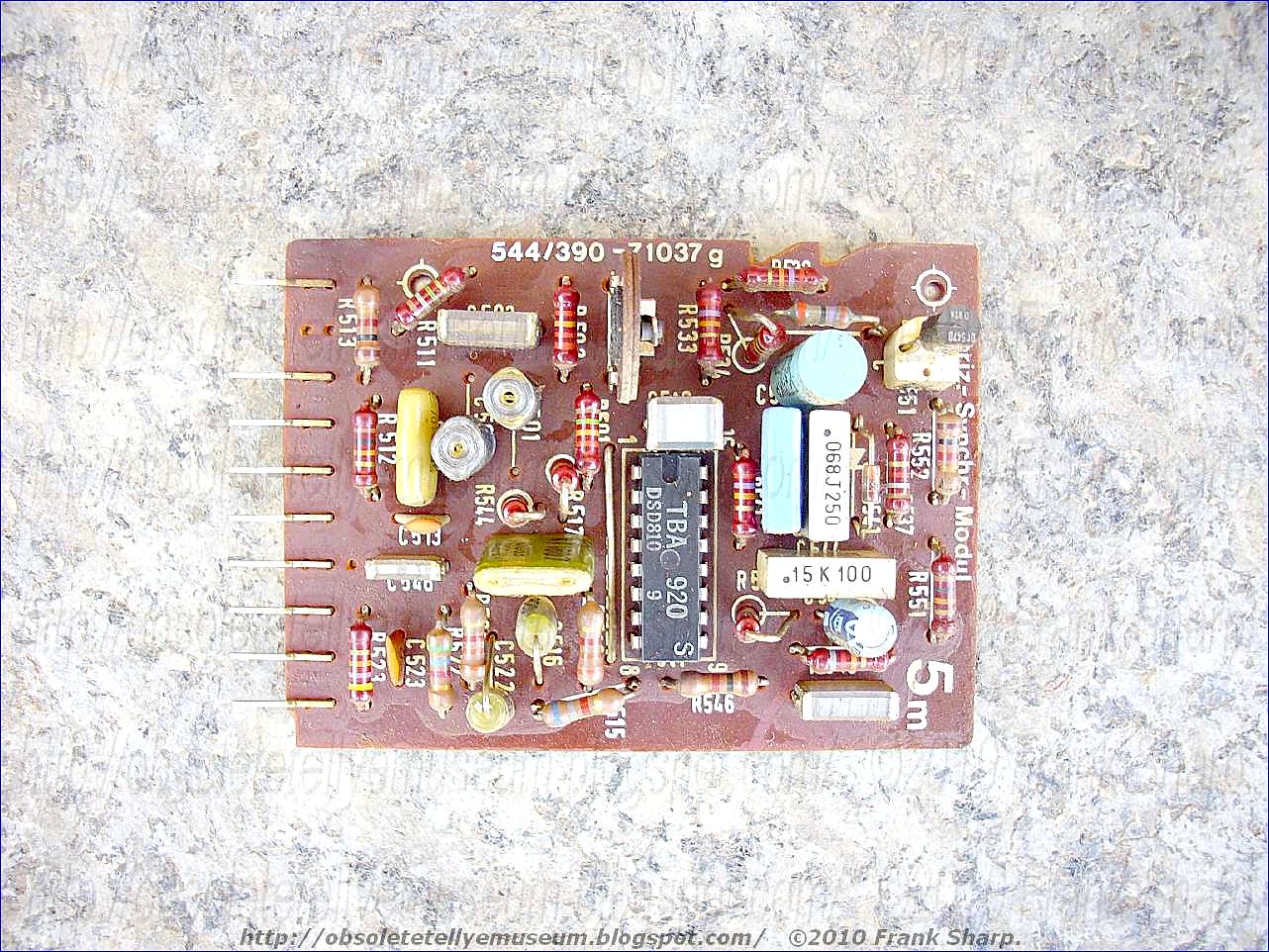
the Grundig SuperColor Models 5011 and 6011. Ty511/Di511 form the
flyback switch, T1 is the input/commutating transformer, C516/7/8
comprise the tuning capacitance, Di518 is the efficiency diode and Ty518
the forward scan thyristor. The scan -correction capacitor Cs is C537.
As can be seen, the line output transformer circuit is quite
conventional. The main complication arises because of the need to
provide width/e.h.t. stabilisation. In a valve line output stage it is a
simple matter to achieve stabilisation by using a v.d.r. in a feedback
circuit to alter the bias on the output pentode. We can't do this with a
transistor line output stage, so we have to operate this in conjunction
with a stabilised supply. There is a subtle but quite simple method of
applying stabilisation to a thyristor line output stage however. As we
have seen, the energy supplied to the output side of the circuit is
provided by the tuning capacitors when they discharge during the flyback
period. During the forward scan they charge via the input coil - or
transformer as it is in practice. Now if we shunt the transformer's
input winding with a transductor we can control the inductance in series
with the tuning capacitors and in consequence the charging time of the
capacitors and hence the power supplied to the output side of the
circuit.
EHT/Width Stabilisation:
The
stabilising transductor in Fig. 6 is Td 1, whose load windings are
connected in series with R504/Di504 across the input winding of T1. The
transductor's control winding is driven by transistor Tr506, which
senses the h.t. voltage (via R506) and the amplitude of the signal at
tag d on the line output transformer. R508 in the transistor's base
circuit enables the e.h.t. to be set to the correct voltage (25kV).
Other Circuit Details:
A fourth winding on Ti feeds the 1.t. rectifier and stabiliser which
provide the supply for the low -power circuits in the receiver. The
trigger pulse winding also feeds a stabilised 1.t. supply circuit
(21V).
EW
pincushion distortion correction is applied by connecting the load
windings of a second transductor (Td2) across a section of the line
output transformer's primary winding. By feeding a field frequency waveform to
the control winding on this transductor the line scanning is modulated
at field frequency. There is a simple but effective safety circuit in
this Grundig line output stage. If the voltage at tag c on the line
output transformer rises above 68V zener diode Di514 conducts,
triggering thyristor Ty511 into conduction with the result that the
cut-out operates. C517 is returned to chassis via a damped coil (L517)
so that the voltage transient when the efficiency diode cuts off is
attenuated. Likewise L512/C512/R512 are added to suppress the voltage
transient when the flyback thyristor Ty511 cuts off. The balancing coil
L516 is included to remove unwanted voltage spikes produced by the
thyristors.
transformer's primary winding. By feeding a field frequency waveform to
the control winding on this transductor the line scanning is modulated
at field frequency. There is a simple but effective safety circuit in
this Grundig line output stage. If the voltage at tag c on the line
output transformer rises above 68V zener diode Di514 conducts,
triggering thyristor Ty511 into conduction with the result that the
cut-out operates. C517 is returned to chassis via a damped coil (L517)
so that the voltage transient when the efficiency diode cuts off is
attenuated. Likewise L512/C512/R512 are added to suppress the voltage
transient when the flyback thyristor Ty511 cuts off. The balancing coil
L516 is included to remove unwanted voltage spikes produced by the
thyristors.
At
the end........This Grundig circuit is representative of the way in
which thyristor line output circuits are used in practice. There are
differences in detail in the thyristor line output stages found in other
setmakers' chassis, but the basic arrangement will be found to be
substantially
Servicing / Throubleshooting / Repairing Thyristor Line Scan Timebases Crt Deflections circuits:
 LARGELY
due to advances in colour c.r.t. scan coil design, the thyristor line
output stage has become obsolete laready in the 1981's.
LARGELY
due to advances in colour c.r.t. scan coil design, the thyristor line
output stage has become obsolete laready in the 1981's.
It
was a very good system to use where the line scan coils require large
peak currents with only a moderate flyback voltage - an intrinsic
characteristic of toroidally wound deflection coils.
it was originally devised by RCA. Many sets fitted with
110°, narrow -neck delta -gun tubes used a thyristor line output stage -
for example those in the Grundig and Saba ranges and the Finlux Peacock
, Indesit, Siemens, Salora, Metz, Nordmende, Blaupunkt, ITT, Seleco,
REX, Mivar, Emerson, Brionvega, Loewe, Galaxi, Stern, Zanussi, Wega,
Philco. The circuit continued to find favour in earlier chassis designed
for use with in -line gun tubes, examples being found in the Grundig
and Korting ranges - also, Indesit, Siemens, Salora, Metz, Nordmende,
Blaupunkt, ITT, Seleco, REX, Mivar, Emerson, Brionvega, Loewe, Galaxi,
Stern, Zanussi, Wega, Philco the Rediffusion Mk. III chassis. Deflection
currents of up to 13A peak -to -peak are commonly encountered with 110°
tubes, with a flyback voltage of only some 600V peak to peak. The
total energy requirement is of the order of 6mJ, which is 50 per cent
higher than modern 110° tubes of the 30AX and S4 variety with their
saddle -wound line scan coils. The only problem with this type of
circuit is the large amount of energy that shuttles back and forth at
line frequency. This places a heavy stress on certain components.
Circuit losses produce quite high temperatures, which are concentrated
at certain points, in particular the commutating combi coil. This leads
to deterioration of the soldered joints around the coil, a common cause
of failure. This can have
a cumulative effect, a high resistance joint increasing the local
heating until the joint becomes well and truly dry -a classic symptom
with some Grundig / Emerson sets. The wound components themselves can be
a source of trouble, due to losses - particularly the combi coil and
the regulating transductor. Later chassis are less prone to this sort of
thing, partly because of the use of later generation, higher efficiency
yokes but mainly due to more generous and better design of the wound
components. The ideal dielectric for use in the tuning capacitors is
polypropylene (either metalised or film). It's a truly won- derful
dielectric - very stable, with very small losses, and capable of
operation at high frequencies and elevated temperatures. It's also
nowadays reasonably inexpensive. Unfortunately many earlier chassis of
thi s type used polyester capacitors, and it's no surprise that they were
inclined to give up. When replacing the tuning capacitors in a
thyristor line output stage it's essential to use polypropylene types -a
good range of axial components with values ranging from 0.001µF to
047µF is available from RS Components, enabling even non-standard values
to be made up from an appropriate combination. Using polypropylene
capacitors in place of polyester ones will not only ensure capacitor
reliability but will also lower the stress on other components by
reducing the circuit losses (and hence power consumption).
s type used polyester capacitors, and it's no surprise that they were
inclined to give up. When replacing the tuning capacitors in a
thyristor line output stage it's essential to use polypropylene types -a
good range of axial components with values ranging from 0.001µF to
047µF is available from RS Components, enabling even non-standard values
to be made up from an appropriate combination. Using polypropylene
capacitors in place of polyester ones will not only ensure capacitor
reliability but will also lower the stress on other components by
reducing the circuit losses (and hence power consumption).
 s type used polyester capacitors, and it's no surprise that they were
inclined to give up. When replacing the tuning capacitors in a
thyristor line output stage it's essential to use polypropylene types -a
good range of axial components with values ranging from 0.001µF to
047µF is available from RS Components, enabling even non-standard values
to be made up from an appropriate combination. Using polypropylene
capacitors in place of polyester ones will not only ensure capacitor
reliability but will also lower the stress on other components by
reducing the circuit losses (and hence power consumption).
s type used polyester capacitors, and it's no surprise that they were
inclined to give up. When replacing the tuning capacitors in a
thyristor line output stage it's essential to use polypropylene types -a
good range of axial components with values ranging from 0.001µF to
047µF is available from RS Components, enabling even non-standard values
to be made up from an appropriate combination. Using polypropylene
capacitors in place of polyester ones will not only ensure capacitor
reliability but will also lower the stress on other components by
reducing the circuit losses (and hence power consumption).
Numerous circuit designs for completely transistorized television
receivers either have been incorporated in commercially available
receivers or have been described in detail in various technical
publications. One of the most troublesome areas in such transistor
receivers, from the point of View of reliability and economy, lies in
the horizontal deflection circuits.
As an attempt to avoid the voltage and current limitations of transistor
deflection circuits, a number of circuits have been proposed utilizing
the silicon controlled rectifier (SCR), a semiconductor device capable
of handling substantially higher currents and voltages than transistors.
The circuit utilizes two bi-directionally conductive switching means
which serve respectively as trace and commutating switches.
Particularly, each of the switching means comprises the parallel
combination of a silicon controlled rectifier (SCR) and a diode. The
commutating switch is triggered on shortly before the desired beginning
of retrace and, in conjunction with a resonant commutating circuit
having an inductor and two capacitors, serves to turn off the trace
switch to initiate retrace. The commutating circuit is also arranged to
turn oft the commutating SCR before the end of retrace.
Circuit Operation:
The
basic thyristor line output stage arrangement used in all these chassis
is shown in Fig. 1 - it was originally devised by RCA. The part to th e
right of the tuning capacitance acts in exactly the same manner as a
transis- tor line output stage, with the scan thyristor Th2 replacing
the transistor. The thyristor is switched on about half way through the
forward scan, the efficiency diode D2 provid- ing the initial part of
the line scan (left-hand side of the screen). The scan coils and line
output transformer (used to generate the e.h.t. plus various other
supply lines and pulse waveforms as required) are a.c. coupled, via the
scan -correction capacitor C5 and C6 respectively. The problem with a
thyristor is that it can be turned on at its gate but not off. To switch
a thyristor off, the current flowing through it must be reduced below a
value known as the hold -on current. This is the main function of the
components on the left-hand side - the line generator, the flyback
thyristor with its parallel diode and the commutat- ing coil. During the
forward scan, the tuning capacitors are charged from the h.t. line via
the input and commutat- ing coils. The line generator produces a pulse
to trigger the flyback thyristor Th1- this occurs just before the actual
flyback. When Thl1 switches on, the junction of the input coil and the
commutating coil is momentarily con- nected to chassis. The tuning
capacitance and the com- mutating coil then resonate, producing a pulse
which draws current via the scan thyristor. Since this current flow is
in the opposite direction to the scan current flow, the two cancel and
the current flowing via the scan thyris- tor falls below the hold -on
current. Th2 is thus switched off, and the scan coils resonate with the
tuning capaci- tance to provide the flyback action. So much for the
basic action. A secondary winding coupled to the input coil produces a
pulse to switch the scan thyristor on, in conjunction with the
shaping/delay network Ll, C4, R1. The tuning capacitors are usually
arranged in the T formation shown to reduce the values required and the
voltages developed across them. In practical circuits the input
and commutating coils are usually combined in a single unit which for
obvious reasons is generally known as the combi coil. The main point not
so far mentioned is stabilisation. There are two approaches to this. In
earlier circuits a transductor was included in parallel with the
e
right of the tuning capacitance acts in exactly the same manner as a
transis- tor line output stage, with the scan thyristor Th2 replacing
the transistor. The thyristor is switched on about half way through the
forward scan, the efficiency diode D2 provid- ing the initial part of
the line scan (left-hand side of the screen). The scan coils and line
output transformer (used to generate the e.h.t. plus various other
supply lines and pulse waveforms as required) are a.c. coupled, via the
scan -correction capacitor C5 and C6 respectively. The problem with a
thyristor is that it can be turned on at its gate but not off. To switch
a thyristor off, the current flowing through it must be reduced below a
value known as the hold -on current. This is the main function of the
components on the left-hand side - the line generator, the flyback
thyristor with its parallel diode and the commutat- ing coil. During the
forward scan, the tuning capacitors are charged from the h.t. line via
the input and commutat- ing coils. The line generator produces a pulse
to trigger the flyback thyristor Th1- this occurs just before the actual
flyback. When Thl1 switches on, the junction of the input coil and the
commutating coil is momentarily con- nected to chassis. The tuning
capacitance and the com- mutating coil then resonate, producing a pulse
which draws current via the scan thyristor. Since this current flow is
in the opposite direction to the scan current flow, the two cancel and
the current flowing via the scan thyris- tor falls below the hold -on
current. Th2 is thus switched off, and the scan coils resonate with the
tuning capaci- tance to provide the flyback action. So much for the
basic action. A secondary winding coupled to the input coil produces a
pulse to switch the scan thyristor on, in conjunction with the
shaping/delay network Ll, C4, R1. The tuning capacitors are usually
arranged in the T formation shown to reduce the values required and the
voltages developed across them. In practical circuits the input
and commutating coils are usually combined in a single unit which for
obvious reasons is generally known as the combi coil. The main point not
so far mentioned is stabilisation. There are two approaches to this. In
earlier circuits a transductor was included in parallel with the  input
coil to vary the impe- dance in series with the tuning capacitance.
This was driven by a transistor which was in turn controlled by feedback
from the line output transformer. A more efficient technique is used in
later circuits, with a current dumping thyristor in series with the
input coil. Practical Circuit As a typical example of the earlier type
of circuit, Fig. 2 shows the thyristor line output stage used in the
Grundig 5010/5011/6010/6011 series. Td1 is the regulating transductor
which is driven by Tr506. Ty511 is the flyback thyristor (commutating
thyristor might be a better name), Ty518 the scan thyristor, Di518 the
efficiency diode and C516/7/8 the tuning capacitance. The scan coils are
cou- pled via C537, while C532 provides coupling between the primary
winding of the line output transformer and chas- sis. A transductor
(Td2) is used for EW raster correction. The combi coil also feeds 1.t.
rectifiers from its secondary windings.
input
coil to vary the impe- dance in series with the tuning capacitance.
This was driven by a transistor which was in turn controlled by feedback
from the line output transformer. A more efficient technique is used in
later circuits, with a current dumping thyristor in series with the
input coil. Practical Circuit As a typical example of the earlier type
of circuit, Fig. 2 shows the thyristor line output stage used in the
Grundig 5010/5011/6010/6011 series. Td1 is the regulating transductor
which is driven by Tr506. Ty511 is the flyback thyristor (commutating
thyristor might be a better name), Ty518 the scan thyristor, Di518 the
efficiency diode and C516/7/8 the tuning capacitance. The scan coils are
cou- pled via C537, while C532 provides coupling between the primary
winding of the line output transformer and chas- sis. A transductor
(Td2) is used for EW raster correction. The combi coil also feeds 1.t.
rectifiers from its secondary windings.
 e
right of the tuning capacitance acts in exactly the same manner as a
transis- tor line output stage, with the scan thyristor Th2 replacing
the transistor. The thyristor is switched on about half way through the
forward scan, the efficiency diode D2 provid- ing the initial part of
the line scan (left-hand side of the screen). The scan coils and line
output transformer (used to generate the e.h.t. plus various other
supply lines and pulse waveforms as required) are a.c. coupled, via the
scan -correction capacitor C5 and C6 respectively. The problem with a
thyristor is that it can be turned on at its gate but not off. To switch
a thyristor off, the current flowing through it must be reduced below a
value known as the hold -on current. This is the main function of the
components on the left-hand side - the line generator, the flyback
thyristor with its parallel diode and the commutat- ing coil. During the
forward scan, the tuning capacitors are charged from the h.t. line via
the input and commutat- ing coils. The line generator produces a pulse
to trigger the flyback thyristor Th1- this occurs just before the actual
flyback. When Thl1 switches on, the junction of the input coil and the
commutating coil is momentarily con- nected to chassis. The tuning
capacitance and the com- mutating coil then resonate, producing a pulse
which draws current via the scan thyristor. Since this current flow is
in the opposite direction to the scan current flow, the two cancel and
the current flowing via the scan thyris- tor falls below the hold -on
current. Th2 is thus switched off, and the scan coils resonate with the
tuning capaci- tance to provide the flyback action. So much for the
basic action. A secondary winding coupled to the input coil produces a
pulse to switch the scan thyristor on, in conjunction with the
shaping/delay network Ll, C4, R1. The tuning capacitors are usually
arranged in the T formation shown to reduce the values required and the
voltages developed across them. In practical circuits the input
and commutating coils are usually combined in a single unit which for
obvious reasons is generally known as the combi coil. The main point not
so far mentioned is stabilisation. There are two approaches to this. In
earlier circuits a transductor was included in parallel with the
e
right of the tuning capacitance acts in exactly the same manner as a
transis- tor line output stage, with the scan thyristor Th2 replacing
the transistor. The thyristor is switched on about half way through the
forward scan, the efficiency diode D2 provid- ing the initial part of
the line scan (left-hand side of the screen). The scan coils and line
output transformer (used to generate the e.h.t. plus various other
supply lines and pulse waveforms as required) are a.c. coupled, via the
scan -correction capacitor C5 and C6 respectively. The problem with a
thyristor is that it can be turned on at its gate but not off. To switch
a thyristor off, the current flowing through it must be reduced below a
value known as the hold -on current. This is the main function of the
components on the left-hand side - the line generator, the flyback
thyristor with its parallel diode and the commutat- ing coil. During the
forward scan, the tuning capacitors are charged from the h.t. line via
the input and commutat- ing coils. The line generator produces a pulse
to trigger the flyback thyristor Th1- this occurs just before the actual
flyback. When Thl1 switches on, the junction of the input coil and the
commutating coil is momentarily con- nected to chassis. The tuning
capacitance and the com- mutating coil then resonate, producing a pulse
which draws current via the scan thyristor. Since this current flow is
in the opposite direction to the scan current flow, the two cancel and
the current flowing via the scan thyris- tor falls below the hold -on
current. Th2 is thus switched off, and the scan coils resonate with the
tuning capaci- tance to provide the flyback action. So much for the
basic action. A secondary winding coupled to the input coil produces a
pulse to switch the scan thyristor on, in conjunction with the
shaping/delay network Ll, C4, R1. The tuning capacitors are usually
arranged in the T formation shown to reduce the values required and the
voltages developed across them. In practical circuits the input
and commutating coils are usually combined in a single unit which for
obvious reasons is generally known as the combi coil. The main point not
so far mentioned is stabilisation. There are two approaches to this. In
earlier circuits a transductor was included in parallel with the  input
coil to vary the impe- dance in series with the tuning capacitance.
This was driven by a transistor which was in turn controlled by feedback
from the line output transformer. A more efficient technique is used in
later circuits, with a current dumping thyristor in series with the
input coil. Practical Circuit As a typical example of the earlier type
of circuit, Fig. 2 shows the thyristor line output stage used in the
Grundig 5010/5011/6010/6011 series. Td1 is the regulating transductor
which is driven by Tr506. Ty511 is the flyback thyristor (commutating
thyristor might be a better name), Ty518 the scan thyristor, Di518 the
efficiency diode and C516/7/8 the tuning capacitance. The scan coils are
cou- pled via C537, while C532 provides coupling between the primary
winding of the line output transformer and chas- sis. A transductor
(Td2) is used for EW raster correction. The combi coil also feeds 1.t.
rectifiers from its secondary windings.
input
coil to vary the impe- dance in series with the tuning capacitance.
This was driven by a transistor which was in turn controlled by feedback
from the line output transformer. A more efficient technique is used in
later circuits, with a current dumping thyristor in series with the
input coil. Practical Circuit As a typical example of the earlier type
of circuit, Fig. 2 shows the thyristor line output stage used in the
Grundig 5010/5011/6010/6011 series. Td1 is the regulating transductor
which is driven by Tr506. Ty511 is the flyback thyristor (commutating
thyristor might be a better name), Ty518 the scan thyristor, Di518 the
efficiency diode and C516/7/8 the tuning capacitance. The scan coils are
cou- pled via C537, while C532 provides coupling between the primary
winding of the line output transformer and chas- sis. A transductor
(Td2) is used for EW raster correction. The combi coil also feeds 1.t.
rectifiers from its secondary windings. 
 Component Problems: The only problem with this type of circuit is the large amount of energy that shuttles back and forth at line frequency.
This places a heavy stress on certain components. Circuit losses
produce quite high temperatures, which are concentrated at certain
points, in particular the combi coil. This leads to deterioration of the
soldered joints around the coil, a common cause of failure. This can
have a cumulative effect, a high -resistance joint increasing the local
heating until the joint becomes well and truly dry -a classic symptom
with some Grundig sets. The wound components themselves can be a source
of trouble, due to losses - particularly the combi coil and the
regulating transductor. Later chassis are less prone to this sort of
thing, partly because of the use of later generation, higher efficiency
yokes but mainly due to more generous and better design of the wound
components. The ideal dielectric for use in the tuning capacitors is
polypropylene (either metalised or film). It's a truly won- derful
dielectric - very stable, with very small losses, and capable of
operation at high frequencies and elevated temperatures. It's also
nowadays reasonably inexpensive. Unfortunately many earlier chassis of
this type used polyester capacitors, and it's no surprise that they were
inclined to give up. When replacing the tuning capacitors in a
thyristor line output stage it's essential to use poly- propylene types
-a good range of axial components with values ranging from 0.001µF to
047µF is available from RS Components, enabling even non-standard values
to be made up from an appropriate combination. Using polypropylene
capacitors in place of polyester ones will not only ensure capacitor
reliability but will
Component Problems: The only problem with this type of circuit is the large amount of energy that shuttles back and forth at line frequency.
This places a heavy stress on certain components. Circuit losses
produce quite high temperatures, which are concentrated at certain
points, in particular the combi coil. This leads to deterioration of the
soldered joints around the coil, a common cause of failure. This can
have a cumulative effect, a high -resistance joint increasing the local
heating until the joint becomes well and truly dry -a classic symptom
with some Grundig sets. The wound components themselves can be a source
of trouble, due to losses - particularly the combi coil and the
regulating transductor. Later chassis are less prone to this sort of
thing, partly because of the use of later generation, higher efficiency
yokes but mainly due to more generous and better design of the wound
components. The ideal dielectric for use in the tuning capacitors is
polypropylene (either metalised or film). It's a truly won- derful
dielectric - very stable, with very small losses, and capable of
operation at high frequencies and elevated temperatures. It's also
nowadays reasonably inexpensive. Unfortunately many earlier chassis of
this type used polyester capacitors, and it's no surprise that they were
inclined to give up. When replacing the tuning capacitors in a
thyristor line output stage it's essential to use poly- propylene types
-a good range of axial components with values ranging from 0.001µF to
047µF is available from RS Components, enabling even non-standard values
to be made up from an appropriate combination. Using polypropylene
capacitors in place of polyester ones will not only ensure capacitor
reliability but will  also
lower the stress on other components by reducing the circuit losses
(and hence power consumption). The thyristors are also liable to fail,
as are their parallel diodes. Earlier devices were less reliable than
their successors. Since all thyristor line output stages operate in the
same way and under similar conditions, the use of later types of
thyristors and diodes in earlier circuits is a matter of mechanical
rather than electrical con- siderations. One important point should be
noted: the scan thyristor is a faster device and often has a higher
voltage rating than the flyback thyristor. The simplest course is to
keep in stock some of the later scan thyristors that incorporate an
efficiency diode - suitable types are the RCA S3900SF and the Telefunken
TD3-800H. The Telefunken device is in a TO66 package (and can be
obtained quite cheaply) while the RCA type is in a TO220 package. Either
type can be used in the scan or flyback positions and can also be used
as a replacement for the regulating thyristor used in later designs
instead of a transductor. Whenever replacing a thyristor in the line
output stage it's good practice to replace the parallel diode at the
same time. Using one of the above recom- mended devices will do this
automatically, since the thyristor and its parallel diode share the same
encapsulation - always remember to remove the old diode when this is a
separate device however, as some can exhibit high -voltage
leakage/breakdown which is not evident from a quite check with the Avo.
Apart from the wound components (including the line output transformer),
the thyristors and their parallel diodes and the tuning capacitors
several other com- ponents are prone to failure. These include the
tripler, scan/flyback rectifier diodes used to provide various supply
lines, surge limiting resistors, the scan coil coup- ling/scan
correction capacitor (replace with a metalised polypropylene type) and
regulator components such as the thyristor in later types and the
transductor driver transistor in earlier circuits.
also
lower the stress on other components by reducing the circuit losses
(and hence power consumption). The thyristors are also liable to fail,
as are their parallel diodes. Earlier devices were less reliable than
their successors. Since all thyristor line output stages operate in the
same way and under similar conditions, the use of later types of
thyristors and diodes in earlier circuits is a matter of mechanical
rather than electrical con- siderations. One important point should be
noted: the scan thyristor is a faster device and often has a higher
voltage rating than the flyback thyristor. The simplest course is to
keep in stock some of the later scan thyristors that incorporate an
efficiency diode - suitable types are the RCA S3900SF and the Telefunken
TD3-800H. The Telefunken device is in a TO66 package (and can be
obtained quite cheaply) while the RCA type is in a TO220 package. Either
type can be used in the scan or flyback positions and can also be used
as a replacement for the regulating thyristor used in later designs
instead of a transductor. Whenever replacing a thyristor in the line
output stage it's good practice to replace the parallel diode at the
same time. Using one of the above recom- mended devices will do this
automatically, since the thyristor and its parallel diode share the same
encapsulation - always remember to remove the old diode when this is a
separate device however, as some can exhibit high -voltage
leakage/breakdown which is not evident from a quite check with the Avo.
Apart from the wound components (including the line output transformer),
the thyristors and their parallel diodes and the tuning capacitors
several other com- ponents are prone to failure. These include the
tripler, scan/flyback rectifier diodes used to provide various supply
lines, surge limiting resistors, the scan coil coup- ling/scan
correction capacitor (replace with a metalised polypropylene type) and
regulator components such as the thyristor in later types and the
transductor driver transistor in earlier circuits.
Basic Fault Conditions: At
one time every engineer must have scratched his head and cursed the
new-fangled idea of the thyristor line output stage. That they are
awkward to service is a fallacy however. The usual symptom of a fault in
the line output stage is the cutout tripping. All chassis that use a
thyristor line timebase incorporate a trip of some sort. The type varies
from chassis to chassis. Early Grundig sets have a mechanical cutout;
the Saba H chassis uses a thyristor and solenoid to open the mains
on/off switch; a common arrangement consists of a thyristor in series
with the h.t, line and a control transistor which shorts the thyristor's
gate and cathode in the event of excessive current demand (this gives
audible tripping at about 2Hz). Some sets incorporate both excess
current and over -voltage trips, but most have just the former.
 There
are two basic fault conditions: when the excess current trip is
activated and the set goes dead, or no e.h.t. with the trip not
activated. The first condition is usually due to a line timebase fault,
the most common being a short-circuit flyback thyristor or its parallel
diode. A straightforward resistance check will sort this out. If this is
not the case, short-circuit the scan thyristor by soldering a wire link
between its anode and cathode. This will prevent any drive to the scan
coils and the line output transformer. If the tripping stops, the fault
could be due to the tripler, the line output transformer, a rectifier
diode fed from a winding on the latter or a short in a circuit supplied
by a scan rectifier diode. If the trip continues to operate and the
flyback thyristor/diode is not the culprit, the most likely causes are
incorrect drive to this thyristor - if possible check with a scope
against the waveform given in the manual - or a rectifier diode fed from
the combi coil. As an example of the latter, Fig. 3 shows the
arrangement used in the Finlux Peacock: the electronic trip will operate
if either D503 or D504 goes short-circuit, a fairly common fault on
these sets. The diodes can also go open-circuit/high resistance to give
the no sound with field collapse symp- tom, but that's another story (
referring to the diodes as D603/4 ). When the set is dead, h.t. is
present and the trip is not activated, suspect the following: the scan
thyristor, the efficiency diode, the line output transformer, the scan -
correction capacitor, or lack of drive to the scan thyristor. Dry
-joints can be the cause of any of these basic fault conditions,
depending on the actual circuit and where the dry -joint has occurred.
The usual symptom is fuzzy verticals and a sawtooth effect on
diagonals. The trip may operate, possibly after period of operation.
These components set up the transductor's operating bias. Linearity
problems are usually caused by the regulator circuit, which can also be
responsible for line "hunting". In the event of lack of width in the
earlier type of circuit, check for dry -joints in the regulator circuit
and suspect the control transistor. Foldover on the left-hand side of
the screen can be caused by an open -circuit flyback diode. Foldover at
the centre of the screen with greatly reduced width is the symptom when
the efficiency diode goes open -circuit - the trip may or may not
operate. Unusual interference patterns on the screen, best viewed with
the contrast control turned to minimum and the brightness control
advanced until a distinctly visible but not over bright white raster is
obtained, can be due to the tripler if there's curved patterning on the
extreme left- hand side of the screen, the regulator clamp diode (Di505
in Fig. 2) if there's curved interference just to the left of centre, or
the flyback thyristor drive circuit if there's a single vertical line
of patterning about four fifths of the way to the right of the screen.
There
are two basic fault conditions: when the excess current trip is
activated and the set goes dead, or no e.h.t. with the trip not
activated. The first condition is usually due to a line timebase fault,
the most common being a short-circuit flyback thyristor or its parallel
diode. A straightforward resistance check will sort this out. If this is
not the case, short-circuit the scan thyristor by soldering a wire link
between its anode and cathode. This will prevent any drive to the scan
coils and the line output transformer. If the tripping stops, the fault
could be due to the tripler, the line output transformer, a rectifier
diode fed from a winding on the latter or a short in a circuit supplied
by a scan rectifier diode. If the trip continues to operate and the
flyback thyristor/diode is not the culprit, the most likely causes are
incorrect drive to this thyristor - if possible check with a scope
against the waveform given in the manual - or a rectifier diode fed from
the combi coil. As an example of the latter, Fig. 3 shows the
arrangement used in the Finlux Peacock: the electronic trip will operate
if either D503 or D504 goes short-circuit, a fairly common fault on
these sets. The diodes can also go open-circuit/high resistance to give
the no sound with field collapse symp- tom, but that's another story (
referring to the diodes as D603/4 ). When the set is dead, h.t. is
present and the trip is not activated, suspect the following: the scan
thyristor, the efficiency diode, the line output transformer, the scan -
correction capacitor, or lack of drive to the scan thyristor. Dry
-joints can be the cause of any of these basic fault conditions,
depending on the actual circuit and where the dry -joint has occurred.
The usual symptom is fuzzy verticals and a sawtooth effect on
diagonals. The trip may operate, possibly after period of operation.
These components set up the transductor's operating bias. Linearity
problems are usually caused by the regulator circuit, which can also be
responsible for line "hunting". In the event of lack of width in the
earlier type of circuit, check for dry -joints in the regulator circuit
and suspect the control transistor. Foldover on the left-hand side of
the screen can be caused by an open -circuit flyback diode. Foldover at
the centre of the screen with greatly reduced width is the symptom when
the efficiency diode goes open -circuit - the trip may or may not
operate. Unusual interference patterns on the screen, best viewed with
the contrast control turned to minimum and the brightness control
advanced until a distinctly visible but not over bright white raster is
obtained, can be due to the tripler if there's curved patterning on the
extreme left- hand side of the screen, the regulator clamp diode (Di505
in Fig. 2) if there's curved interference just to the left of centre, or
the flyback thyristor drive circuit if there's a single vertical line
of patterning about four fifths of the way to the right of the screen.The aim of this article has been to provide a general guide to servicing rather than to list faults common to particular models. Much useful information on individual
chassis with thyristor line output stages has appeared in previous issues of Obsolete Technology Tellye !- refer to the following as required: Search with the tag Thyristors at the bottom of the post to select all posts with this argument on various fabricants.
Isolated mains chassis thyristor technology:
 A supply circuit for television receivers in which power source isolation is effected via a backward transformer. For the sake of achieving an insusceptibility to interferences, the operating frequency is equal to the line frequency. According to the invention, the supplied energy is controlled by varying the switch-on time during one period of the line frequency, in that the disconnecting time position is changed with the aid of a thyristor switching stage.
1. A su
an input transformer having a secondary winding connected to the horizontal output stage for providing the energy required thereby and a primary winding adapted for connection to the power source and being electrically isolated from the secondary winding and the horizontal output stage;
electronic switch means connected in series with the primary winding of the transformer;
first switching control means for switching on the electronic switch means as a function of line frequency; and
second switching control means for switching off the electronic switch means as a function of the energy required by the horizontal output stage, whereby the supply circuit provides the horizontal output stage with the required energy from the power source while also electrically isolating the horizontal output stage from the power source.
2. A supply circuit as described in claim 1, wherein the electronic switch means comprises a thyristor stage.
3. A supply circuit as described in claim 1, wherein the thyristor stage comprises a thyristor and a diode connected in inverse parallel manner, the gate electrode of the thyristor being connected to the first switching control means for turning on the thyristor.
4. A supply circuit as described in claim 3, wherein the first switching control means includes a horizontal deflection oscillator.
5. A supply circuit as described in claim 4, additionally comprising an isolation transformer connected between the thyristor gate and the horizontal deflection oscillator.
6. A supply circuit as described in claim 2, wherein the second switching control means comprises a series resonant circuit having an adjustable resonant frequency, said circuit being connected in parallel with the thyristor stage for causing commutation of the current in the thyristor stage.
7. A supply circuit as described in claim 6, wherein the series resonant circuit includes a transductor having a control winding, and the second switching control means additionally comprises a control circuit adapted to receive a signal from a high voltage transformer of the horizontal output stage and to provide in response thereto an output signal to the control winding of the transductor, said output signal varying in accordance with the signal from the high voltage transformer for varying the inductance of the transductor.
Description:
The present invention relates to a supply circuit for a television receiver in which, for effecting isolation of the power source , an input transformer serving the horizontal or line output stage, is operated as a backward transformer and in which, within the horizontal (line) output stage, there are taken off further voltages required for operating the television receiver.
Owing to the various attachments which are capable of being operated in connection with a television receiver, it has increasingly become necessary, for safety reasons, to provide for isolation of the power source the television receiver.
In conventional types of circuits employing backward transformers for effecting the source isolation, it is customary to control the energy supply by way of inserting a transistorized control stage.
The use of transistors in such a circuit part, however, has proved to be problematic owing to the fact that the transistors are sensitive to any case of exceeding the prescribed operational values.
From the German technical journal "Funkschau" 1975, No. 5, page 40 there has already become known a
 circuit employing a thyristor switching stage for controlling the energy supply. In this circuit, the operating frequency of the thyristor switching stage is dependent upon the operating frequency of the subsequently following horizontal (line) output stage; accordingly, there is concerned a so-called free-running switching stage.
In order to eliminate as far as possible the danger of noise influences as linked thereto, the actually advantageous thyristor switching stage involves a rather considerable investment.,
It is the object of the invention, therefore, with respect to a circuit of the type mentioned hereinbefore, to avoid the described disadvantages of the conventional arrangments, and to safeguard an operationally reliable control of the supplied energy.
This object is achieved in that the energy as supplied to the horizontal (line) output stage is capable of being controlled by means of a thyristor switching stage arranged in series with the primary winding of the input transformer, with first switching means, in dependence upon the line frequency, switching the thyristor switching stage to the conducting state, and with further switching means serving to block the thyristor switching stage in dependence upon the required energy.
Further details and advantages of the invention may be taken from the patent claims as well as from the following description of the accompanying drawing.
FIG. 1 shows one example of embodiment of the invention.
 The horizontal output (final) stage 20 is connected via the input transformer 10 including the primary winding 11 and the secondary winding 12, to the source of supply current B.
As an example relating to the horizontal output (final) stage there is shown in FIG. 1 a thyristor circuit as described in the company publication "Deflection, Power Supply and Correction Circuits for 110° Color Picture Tube A67 - 150x with Toroidal Yoke", No. 59-72-E of Standard Elektrik Lorenz AG, dated Apr. 20, 1972.
By the input transformer 10, the horizontal output stage 20 is galvanically separated from the source of supply current B, i.e. also from the power source. The most important function units of the horizontal output stage will now be mentioned briefly hereinafter.
The reference numeral 21 indicates the schematically shown combined inductive component consisting of deflecting coils and EHT transformer.
The switching stage 22 consisting of a thyristor and of an anti-parallel connected diode, represents the stage controlling the line sweep while the similarly designed switching stage 23 is the so-called commutating switch.
Between these two switching stages there is connected the commutating inductive component 25 and the commutating capacitor consisting of a capacitor combination 26.
 The electrical energy as required in the deflection circuit and the remaining circuit parts not shown herein, and connected to the horizontal output stage 20, is fed to this horizontal output (final) stage 20 in the way according to the invention to be explained hereinafter.
The primary circuit of the inductive component 10 designed as an input transformer, is connected to the supply source B, at the "plus" and "minus" terminals of which the rectified power source voltage is available. The input transformer 10 comprises the primary winding 11 and the secondary winding 12. In series with the primary winding 11 there is arranged a thyristor switching stage consisting of a thyristor 13 and of a diode 14, with both the thyristor and the diode being connected antiparallel.
The thyristor 13 is controlled in this case by inserting an isolating transformer 19, by the horizontal oscillator 18, which means to imply that the operating frequency of the supply circuit including the input transformer 10 is identical to that of the horizontal final stage 20.
The switch-on time position, i.e. the one at which the thyristor 13 is switched to the conducting state, is determined by the control pulse from the horizontal oscillator 18.
Disconnection of the thyristor 13 or switching to the non-conducting state, is effected in the usual way by a current reversal during the time interval in which e.g. the commutating switch 23 is blocked. This is effected by the series resonant circuit arranged in parallel with the thyristor switching stage, including the capacitor 16 and the inductive component 15, in cooperation with the diode 14. This disconnecting time position or the time position at which the thyristor 13 is switched to the non-conducting state, is determined by the resonant frequency of the series-resonant circuit. Accordingly, at a constant switch-on time position, it is possible to determine the period of time during which the thyristor 13 is switched to the conducting state, by varying the resonant frequency and, consequently, by shifting the time position at which the thyristor 13 is switched to the non-conducting state. The period of time during which the thyristor 13 is switched to the conducting state, and, consequently, the period of time of the current flow, however, are decisive for the amount of energy capable of being taken off the input transformer 10 or the secondary winding 12 respectively.
The aforementioned variation of the resonant frequency of the series-resonant circuit, may be carried out, on principle, by a capacitance variation of the capacitor 16, as well as by changing the inductance 15, or else by both.
In the shown example of embodiment there has been chosen a variation of the inductance, in which case, as an inductive component, a transductor is inserted in such a way that its operating winding is in series with the capacitor 16. Transductor 15 provides an inductance that varies in accordance with a DC signal applied thereto. If now, in accordance with stipulations, the energy supply is to be controlled in dependence upon the energy requirement, a corresponding control circuit will have to be provided for.
The energy consumed in the horizontal final stage can be measured by the value of the voltage of the kick-back pulse at the EHT transformer. In order to obtain this value, a tap 211 is schematically shown at the inductive component 21 of the horizontal final stage 20. This tap is connected to a control circuit 17.
As already mentioned, a transductor 15 is used as the adjustable inductive component of the series resonant circuit, whose inductance is capable of being varied by varying the current or voltage as applied to the control winding. At the same time, the transductor effects a galvanic separation. The control circuit 17 into the output circuit of which, according to FIG. 1, there is connected the control winding of the transductor 15, thus serves to convert the value of the voltage of the kickback pulse available as the input or control quantity, into a corresponding value for adjusting the inductive component 15.
 Control circuits, such as e.g. 17, are on principle generally known to those skilled in the art and, therefore, do not need to be explained in detail herein, especially since the circuit-technical embodiment thereof is not germane to the present invention. An example of a control circuit that may be used for circuit 17 is shown in the publication previously referred to and entitled: "Deflection, Power Supply and Correction Circuits for 110° Color Picture Tube A67 - 150x with Toroidal Yoke".
It should still be mentioned that the input transformer 10 is operated as a backward transformer comprising a correspondingly polarized diode 24 in the secondary circuit, which is of advantage for reasons of dimensioning the input transformer 10.
Owing to the various attachments which are capable of being operated in connection with a television receiver, it has increasingly become necessary, for safety reasons, to provide for isolation of the power source the television receiver.
In conventional types of circuits employing backward transformers for effecting the source isolation, it is customary to control the energy supply by way of inserting a transistorized control stage.
The use of transistors in such a circuit part, however, has proved to be problematic owing to the fact that the transistors are sensitive to any case of exceeding the prescribed operational values.
From the German technical journal "Funkschau" 1975, No. 5, page 40 there has already become known a
In order to eliminate as far as possible the danger of noise influences as linked thereto, the actually advantageous thyristor switching stage involves a rather considerable investment.,
It is the object of the invention, therefore, with respect to a circuit of the type mentioned hereinbefore, to avoid the described disadvantages of the conventional arrangments, and to safeguard an operationally reliable control of the supplied energy.
This object is achieved in that the energy as supplied to the horizontal (line) output stage is capable of being controlled by means of a thyristor switching stage arranged in series with the primary winding of the input transformer, with first switching means, in dependence upon the line frequency, switching the thyristor switching stage to the conducting state, and with further switching means serving to block the thyristor switching stage in dependence upon the required energy.
Further details and advantages of the invention may be taken from the patent claims as well as from the following description of the accompanying drawing.
FIG. 1 shows one example of embodiment of the invention.
The horizontal output (final) stage 20 is connected via the input transformer 10 including the primary winding 11 and the secondary winding 12, to the source of supply current B. As an example relating to the horizontal output (final) stage there is shown in FIG. 1 a thyristor circuit as described in the company publication "Deflection, Power Supply and Correction Circuits for 110° Color Picture Tube A67 - 150x with Toroidal Yoke", No. 59-72-E of Standard Elektrik Lorenz AG, dated Apr. 20, 1972.
By the input transformer 10, the horizontal output stage 20 is galvanically separated from the source of supply current B, i.e. also from the power source. The most important function units of the horizontal output stage will now be mentioned briefly hereinafter.
The reference numeral 21 indicates the schematically shown combined inductive component consisting of deflecting coils and EHT transformer.
The switching stage 22 consisting of a thyristor and of an anti-parallel connected diode, represents the stage controlling the line sweep while the similarly designed switching stage 23 is the so-called commutating switch.
Between these two switching stages there is connected the commutating inductive component 25 and the commutating capacitor consisting of a capacitor combination 26.
The primary circuit of the inductive component 10 designed as an input transformer, is connected to the supply source B, at the "plus" and "minus" terminals of which the rectified power source voltage is available. The input transformer 10 comprises the primary winding 11 and the secondary winding 12. In series with the primary winding 11 there is arranged a thyristor switching stage consisting of a thyristor 13 and of a diode 14, with both the thyristor and the diode being connected antiparallel.
The thyristor 13 is controlled in this case by inserting an isolating transformer 19, by the horizontal oscillator 18, which means to imply that the operating frequency of the supply circuit including the input transformer 10 is identical to that of the horizontal final stage 20.
The switch-on time position, i.e. the one at which the thyristor 13 is switched to the conducting state, is determined by the control pulse from the horizontal oscillator 18.
Th
e aforementioned variation of the resonant frequency of the series-resonant circuit, may be carried out, on principle, by a capacitance variation of the capacitor 16, as well as by changing the inductance 15, or else by both. In the shown example of embodiment there has been chosen a variation of the inductance, in which case, as an inductive component, a transductor is inserted in such a way that its operating winding is in series with the capacitor 16. Transductor 15 provides an inductance that varies in accordance with a DC signal applied thereto. If now, in accordance with stipulations, the energy supply is to be controlled in dependence upon the energy requirement, a corresponding control circuit will have to be provided for.
The energy consumed in the horizontal final stage can be measured by the value of the voltage of the kick-back pulse at the EHT transformer. In order to obtain this value, a tap 211 is schematically shown at the inductive component 21 of the horizontal final stage 20. This tap is connected to a control circuit 17.
As already mentioned, a transductor 15 is used as the adjustable inductive component of the series resonant circuit, whose inductance is capable of being varied by varying the current or voltage as applied to the control winding. At the same time, the transductor effects a galvanic separation. The control circuit 17 into the output circuit of which, according to FIG. 1, there is connected the control winding of the transductor 15, thus serves to convert the value of the voltage of the kickback pulse available as the input or control quantity, into a corresponding value for adjusting the inductive component 15.
It should still be mentioned that the input transformer 10 is operated as a backward transformer comprising a correspondingly polarized diode 24 in the secondary circuit, which is of advantage for reasons of dimensioning the input transformer 10.
LOEWE CT5067U CHASSIS C5000 20AX INTEGRAL THYRISTOR-RECTIFIER DEVICEA semiconductor switching device comprising a silicon controlled rectifier (SCR) and a diode rectifier integrally connected in parallel with the SCR in a single semiconductor body. The device is of the NPNP or PNPN type, having gate, cathode, and anode electrodes. A portion of each intermediate N and P region makes ohmic contact to the respective anode or cathode electrode of the SCR. In addition, each intermediate region includes a highly conductive edge portion. These portions are spaced from the adjacent external regions by relatively low conductive portions, and limit the conduction of the diode rectifier to the periphery of the device. A profile of gold recombination centers further electrically isolates the central SCR portion from the peripheral diode portion.
LOEWE CT5067U CHASSIS C5000 20AX LINE DEFLECTION WITH THYRISTOR SWITCH TECHNOLOGY OVERVIEW.
(Thyristor Horizontalsteuerung UND ABLENKUNG)


Description:
1. A horizontal deflection circuit for generating the deflection current in the deflection coil of a television picture tube wher
Description:
The present invention relates to a horizontal deflection circuit for generating the deflection current in the deflection coil of a television picture tube wherein a first switch controls the horizontal sweep, and wherein a second switch in a so-called commutation circuit with a commutating inductor and a commutating capacitor opens the first switch and, in addition, controls the energy transfer from a dc voltage source to an input inductor. German Aus
As can be seen, such a circuit needs two different, separate inductive elements, it being known that inductive elements are expensive to manufacture and always have a certain volume determined by the electrical properties required.
The object of the invention is to reduce the amount of inductive elements required.
The invention is characterized in that the input inductor and the commutating inductor are combined in a unit designed as a transformer which is proportioned so that the open-circuit inductance of the transformer is essentially equal to the value of the input inductor, while the short-circuit inductance of the transformer is essentially equal to the value of the commutating inductor, and that the second switch is connected in series with the dc voltage source and a first winding of the transformer.
This solution has an added advantage in that, in mass production, both the open-circuit and the short-circuit inductance are reproducible with reliability.
According to another feature of the invention, the electrical isolation between the windings of the transformer is such that the transformer operates as an isolation transformer between the supply and the subcircuits connected to a second winding or to additional windings of the transformer. In this manner, the transformer additionally provides reliable mains isolation.
According to a further feature of the invention, the second switch is connected between ground and that terminal of the first winding of the transformer not connected to the supply potential. This simplifies the control of the switch.
According to a further feature of the invention, to regulate the energy supply, the second winding of the transf
The advantage gained by this measure lies in the fact that the control takes place on the side separated from the mains, so no separate isolation device is required for the gating of the third switch. Further details and advantages will be apparent from the following description of the accompanying drawings and from the claims. In the drawings,
FIG. 1 is a basic circuit diagram of the arrangement disclosed in German Auslegeschrift (DT-AS) No. 1,537,308;
FIG. 2 shows a first embodiment of the horizontal deflection circuit according to the invention, and
FIG. 3 shows a development of the horizontal deflection circuit according to the invention.
FIG. 1 shows the essential circuit elements of the horizontal deflection circuit known from the German Auslegeschrift (DT-AS) No. 1,537,308 referred to by way of introduction.
Connected in series with a dc voltage source UB is an input inductor Le and a bipolar, controlled switch S2. In the following, this switch will be referred to as the "second switch"; it is usually called the "commutating switch" to indicate its function.
In known circuits, the second switch S2 consists of a controlled rectifier and a diode connected in inverse parallel.
The second switch S
FIGS. 2 and 3 show the horizontal deflection circuit modified in accordance with the present invention. Like circuit elements are designated by the same reference characters as in FIG. 1.
FIG. 2 shows the basic principle of the invention. The two inductors Le and Lk of FIG. 1 have been replaced by a transformer U. To be able to serve as a substitute for the two inductors Le and Lk, the transformer must be proportioned in a special manner. Regardless of the turns ratio, the open-circuit inductance of the transformer is chosen to be essentially equal to the value of the input inductor Le, and the short-circuit inductance of the transformer is essentially equal to the value of the commutating inductor Lk.
To permit the second switch S2 to be utilized for the connection of the dc voltage source UB, it is included in the circuit of that winding U1 of the transformer connected to the dc voltage UB.
In principle, it is of no consequence for the operation of the switch S2 whether it is inserted on
In compliance with pertinent safety regulations, the transformer U may be designed as an isolation transformer and can thus provide mains separation, which is necessary for various reasons. It is known from German Offenlegungschrift (DT-OS) No. 2,233,249 to provide dc isolation by designing the commutating inductor as a transformer, but this measure is not suited to attaining the object of the present invention.
If the energy to be taken from the dc voltage source is to be controlled as a function of the energy needed in the horizontal deflection circuit and in following subcircuits, the embodiment of the horizontal deflection circuit of FIG. 3 may be used.
The circuit including the winding U2 of the transformer U contains a third controlled switch S3, which, too, is inserted on the grounded side of the winding U2 for the reasons mentioned above. This third switch S3, just as the second switch S2, is operated at the frequency of a horizontal oscillator HO, but a control circuit RS whose input l is fed with a controlled variable is inserted between the oscillator and the switch S3. Depending on this controlled variable, the controlled rectifier of the third switch S3 can be caused to turn on earlier. A suitable controlled variable containing information on the energy consumption is, for example, the flyback pulse capable of being taken from the high voltage generating circuit (not shown). Details of the operation of this kind of energy control are described in applicant's German Offenlegungsschrift (DT-OS) No. b 2,253,386 and do not form part of the present invention.
With mains isolation, the additional, third switch S3 shown here has the advantage of being on the side isolated from the mains and eliminates the need for an isolation device in the control lead of the controlled rectifier.
As an isolation transformer, the transformer U may also carry additional windings U3 and U4 if power is to be supplied to the audio output stage, for example; in addition, the first switch S1 may be gated via such an additional winding.
The points marked at the windings U1 and U2 indicate the phase relationship between the respective voltages. Connected in parallel with the winding U1 and the second switch S2 is a capacitor CE which completes the circuit for the horizontal-frequency alternating current; this serves in particular to bypass the dc voltage source or the electrolytic capacitors contained therein.
LOEWE CT5067U CHASSIS C5000 20AX Electron beam deflection circuit including thyristors Further Discussion and deepening of knowledge, Thyristor horizontal output circuits:

2. A deflection circuit as claimed in claim 1, wherein said amount of additional current is greater than or equal to 5 per cent of the peak-to-peak value of the current flowing through the deflection winding.
3. A deflection circuit as claimed in claim 1, wherein said means for drawing a substantial amount of additional current through said first switching means comprises a resistor connected in parallel to said first capacitor.
4. A deflection circuit as claimed in claim 1, wherein said means for drawing an additional current is formed by connecting said first and second energy sources in series so that the current charging said reactive circuit means forms the said additional current.
5. A deflection circuit as claimed in claim 1, further including a series combination of an autotransformer winding and a second high-value capacitor, said combination being connected in parallel to said first switching means, wherein said autotransformer comprises an intermediate tap located between its terminals respectively connected to said first switching means and to said second capacitor, said tap delivering, during said trace portion, a suitable DC supply voltage lower than the voltage across said second capacitor; and wherein said means for drawing a substantial amount of additional current comprises a load to be fed by said supply voltage and having one terminal connected to ground; and further controllable switching means controlled to conduct during at least part of said trace portion and to remain cut off during said retrace portion, said further switching means being connected between said tap and the other terminal of said load.
Description:
 The present invention relates to electron beam deflection circuits including thyristors, such as silicon controlled rectifiers and relates, in particular, to horizontal deflection circuits for television receivers.
 The present invention constitutes an improvement in the circuit described in U.S. Pat. No. 3,449,623 filed on Sept. 6, 1966, this circuit being described in greater detail below with reference to FIGS. 1 and 2 of the accompanying drawings. A deflection circuit of this type comprises a first thyristor switch which allows the conenction of the horizontal deflection winding to a constant voltage source during the time interval used for the transmisstion of the picture signal and for applying this signal to the grid of the cathode ray tube (this interval will be termed the "trace portion" of the scan), and a second thyristor switch which provides the forced commutation of the first one by applying to it a reverse current of equal amplitude to that which passes through it from the said voltage source and thus to initiate the retrace during the horizontal blanking interval.
A undirectional reverse blocking triode type thyristor or silicon controlled rectifier (SCR), such as that used in the aformentioned circuit, requires a certain turn-off time between the instant at which the anode current ceases and the instant at which a positive bias may be applied to it without turning it on, due to the fact that there is still a high concentration of free carriers in the vicinity of the middle junction, this concentration being reduced by a process of recombination independently from the reverse polarity applied to the thyristor. This turn-off time of the thyristor is a function of a number of parameters such as the junction temperature, the DC current level, the decay time of the direct current, the peak level of the reverse current applied, the amplitude of the reverse anode to cathode voltage, the external impedance of the gate electrode, and so on, certain of these varying considerably from one thyristor to another.
In horizontal deflection circuits for television receivers, the flyback or retrace time is limited to approximately 20 percent of the horizontal scan period, the retrace time being in the case of the CCIR standard of 625 lines, approximately 12 microseconds and, in the case of the French standard of 819 lines, approximately 9 microseconds. During this relatively short interval, the thyristor has to be rendered non-conducting and the electron beam has to be returned to the origin of the scan. The first thyristor is blocked by means of a series resonant LC circuit which is subject to a certain number of restrictions (limitations as to the component values employed) due to the fact that, inter alia, it simultaneously determines the turn-off time of the circuit which blocks the thyristor and it forms part of the series resonant circuit which is to carry out the retrace. To obtain proper operation of the deflection circuit of the aforementioned Patent, especially when used for the French standard of 819 lines per image, the values of the components used have to subject to very close tolerances (approximately 2%), which results in high costs.
The improved deflection circuit, object o
According to the invention, there is provided an electron beam deflection circuit for a cathode ray tube with electromagentic deflection by means of a sawtooth current waveform having a trace portion and a retrace portion, said circuit comprising: a deflection winding; a first source of electrical energy formed by a first capacitor; first controllable switching means comprising a parallel combination of a first thyristor and a first diode, connected together to conduct in opposite directions, for connecting said winding to said first source during said trace portion when said first switching means is turned on; a second source of electrical energy including a first inductive energy storage means coupled to a voltage supply; reactive circuit means including a combination of inductive and capacitive reactances for storing the energy supplied by the said second source; a second controllable switching means, substantially identical with the first one, for completing a circuit including said reactive circuit means and said first switching means, when turned on, so as to pass through said first thyristor an oscillatory current in the opposite direction to that which passes through it from said first source and to turn it off after these two currents cancel out, the oscillatory current then flowing through said first diode for an interval termed the circuit turn-off time which has to be greater than the turn-off time of said first thyristor; and means for drawing duing at least a part of said trace portion a substantial amount of additional current from said first switching means in the direction of conduction of said first diode, whereby said circuit turn-off time is lengthened in proportion to the amount of said additional current, without altering the values of the reactances in the reactive circuit by shifting the waveform of the current flowing through said first switching means towards the negative by an amount equal to that of said additional current.
A further object of the invention consists in using the supplementary current in the recovery diode of the first switching means to produce a DC voltage which may be used as a power supply for the vertical deflection circuit of the television receiver, for example.
The invention will be better understood and other features and advantages thereof will become apparent from the following description and the accompanying drawings, given by way of example, and in which:
FIG. 1 is a schematic circuit diagram partially in bloc diagram form of a prior art deflection circuit according to the aforementioned Patent;
FIG. 2 shows waveforms of currents and voltages generated at various points in the circuit of FIG. 1;FIG. 3 is a schematic diagram of a deflection circuit according to the invention which allows the principle of the improvement to be explained;
FIG. 4 is a diagram of the waveforms of the current through the first switching means 4, 5 of the circuit of FIG. 3;
FIG. 5 is a circuit diagram of another embodiment of the circuit according to the invention;
FIG. 6 is a schematic representation of the preferred embodiment of the circuit according to the invention; and
FIG. 7 shows voltage waveforms at various points of the high voltage autotransformer 21 of FIG. 6.
In all these Figures the same reference numerals refer to the same components.
FIG. 1 shows the horizontal deflection circuit described and claimed in the U.S. Pat. No. 3,449,623 mentioned above, which comprises a first source of electrical energy in the shape of a first capacitor 2 having a high capacitance C 2 for supplying a substantially constant voltage Uc 2 across its terminals. A first terminal of the first capacitor 2 is connected to ground, whilst its second terminal which supplies a positive voltage is connected to one of the terminals of a horizontal deflection winding shown as a first inductance 1. A first switching means 3, consisting of a first reverse blocking triode thyristor 4 (SCR) and a first recovery diode 5 in parallel, the two being interconnected to conduct current in opposite directions, is connected in parallel with the series combination formed by the deflection winding 1 and the first capacitor 2. The assembly of components 1, 2, 4 and 5 forms the final stage of the horizontal deflection circuit in a television receiver using electromagnetic delfection.The deflection circuit also includes a drive stage for this final stage which here controls the turning off of the first thyristor 4 to produce the retrace or fly-back portion of the scan during the line-blanking intervals i.e. while the picture signal is not transmitted. This driver stage comprises a second voltage source in the shape of a DC power supply 6 which delivers a constant high voltage E. The negative terminal of the power supply 6 is connected to ground and its positive terminal to one of the terminals of a second inductance 7 of relatively high value, which draws a substantially lineraly varying current from the power supply 6 to avoid its overloading. The other terminal of th
The respective values of the third inductance 8 (L 8 ) and of the second capacitor 9 (C 9 ) are principally selected so that, on the one hand, one half-cycle of oscillation of the first series resonant circuit L 8 - C 9 , (i.e. π √ L 8 . C 9 ) is longer than the turn-off time of the first thyristor 4, but still is as short as possible since this time interval determines the speed of the commutation of the thyristor 4, and, on the other hand, one half-cycle of oscillation of another series resonant circuit formed by L 1 , L 8 and C 9 , i.e. π √ (L 1 + L 8 ) . C 9 , is substantially equal to the required retrace time interval (i.e. shorter than the horizontal blanking interval).
The gate (control electrode) of the second thyristor 11 is coupled to the output of the horizontal oscillator 13 of the television receiver by means of a first pulse transformer 14 and a first pulse shaping circuit 15 so that it is fed short triggering pulses which are to turn it on.
The gate of the first thyristor 4 fed with signals of a substantially rectangular waveform which are negative during the horizontal blanking intervals, is coupled to a winding 16 by means of a second pulse shaping circuit 17, the winding 16 being magnetically coupled to the second inductance 7 to make up the secondary winding of a transformer of which the inductance 7 forms the primary winding. It will be noted here that it is also possible to couple the secondary winding 16 magnetically to a primary winding connected to a suitable output (not shown) of the horizontal oscillator 13.
The operation of a circuit of this type will be explained below with reference to FIG. 2 which shows the waveforms at various points in the circuit of FIG. 1 during approximately one line period.
FIG. 2 is not to scale since one line period (t 7 - t 0 ) is equal to 64 microseconds in the case of 625 lines and 49 microseconds in the case of 819 lines, while the durations of the respective horizontal blanking intervals are approximately 12 and 9.5 microseconds.Waveform A shows the form of the current i L1 passing through deflection winding 1, this current having a sawtooth waveform substantially linear from t 0 to t 3 and from t 5 to t 7 , and crossing zero at time instants t 0 and t 7 , and reaching values of + I 1m and - I 1m , at time instants t 3 and t 5 respectively, these being its maximum positive and negative amplitudes.
During the second half of the trace portion of the horizontal deflection cycle, that is to say from t 0 to t 3 , the thyristor 4 of the first switching means 3 is conductive and makes the high value capacitor 2 discharge through the deflector winding 1, which has a high inductance, so that current i L1 increases linearly.
A few microseconds (5 to 8 μ s) before the end of the trace portion, i.e. at time instant t 1 , the trigger of the second thyristor 11 receives a short voltage pulse V G11 which causes it to turn on as its anode is at this instant at a positive potential with respect to ground, which is due to the charging of the second capacitor 9 through inductances 7 and 8 by the voltage E from the power supply 6.
When thyristor 11 is made conductive at time t 1 , on the one hand, inductance 7 is connected between ground and the voltage source 6 and a linearly increasing current flows through it and, on the other hand, the reactive circuit 8, 9 forms a loop through the second and first switching means 10 and 3, thus forming a resonant circuit which draws an oscillatory current i 8 ,9 of frequency ##EQU1##
This oscillatory current i 8 ,9 will pass through the first switching means 3, i.e. thyristor 4 and diode 5, in the opposite direction to that of current i L1 . Since the frequency f 1 is high, current i 8 ,9 will increase more rapidly than i L1 and will reach the same level at time t 2 , that is to say i 8 ,9 (t 2 ) = -i L1 (t 2 ) and these currents will cancel out in the thyristor 4 in accordance with the well known principle of forced commutation. After time instant t 2 , current i 8 ,9 continues to increase more rapidly than i L1 , but the difference between them (i 8 ,9 - i L1 ) passes the diode 5 (see wave form B) until it becomes zero at time instant t 3 which is the turn off time instant of the first switching means 3, at which the retrace begins.
The interval between the time instant t 2 and t 3 , i.e. (t 3 -t 2 ), during which diode 5 is conductive and the thyristor is reverse biased will be termed in what follows the circuit turn-off time and it should
The retrace which stated at time t 3 takes place during one half-cycle of the resonant circuit formed by reactances L 1 , L 8 and C 9 , i.e. during the interval between t 3 and t 5 . In the middle of this interval i.e. at time instant t 4 , both i L1 (waveform A) and i 8 ,9 (waveform D) pass through zero and change their sign, whereas the voltage at the terminals of the first switching means 3 (V 3 , waveform E) passes through a maximum. Thus, from t 4 onwards, thyristor 11 will be reverse biased and diode 12 will conduct the current from the resonant circuit 1, 8 and 9 in order to turn the second thyristor 11 off.
At time instant t 5 , when current i L1 has reached - I 1m and when voltage v 3 falls to zero, diode 5 of the first switching means 3 becomes conductive and the trace portion of scan begins.
Current i 8 ,9 nevertheless continues to flow in the resonant circuit 8, 9 through diodes 5 and 12, which causes a break to appear in waveform D at t 5 , and a negative peak to appear in waveform D and a positive one in waveform B in the interval between t 5 and t 6 , these being principally due to the distributed capacities of coil 1 or to an eventual capacitor (not shown) connected in parallel to the first switching means 3.
At time instant t 6 , diode 12 of the second switching means 10 ceases to conduct after having allowed thyristor 11 time to become turned off completely.
The level of current i 8 ,9 at time instant t 5 (i.e. I c ) as well as the negative peak I D12 in i 8 ,9 and the positive peak I D5 in i 5 depend on the values of L 8 and C 9 in the same way as does the turn-off time of the circuit (t 3 - t 2 ). If, for example, L 8 and C 9 , are increased I D5 increases towards zero and this could cause diode 5 to be cut off in an undesirable fashion. I c also increases towards zero, which is liable to cause diode 12 to be blocked and thyristor 11 to trigger prematurely.
From the foregoing it can be clearly seen that the choice of values for L 8 and C 9 is subject to four limitations which prevent the values from being increased to lengthen the turn-off time of the driver circuit of first switching thyristor 4 so as to forestall its spurious triggering.
Waveform F shows the voltage v G4 obtained at the gate of thyristor 4 from the secondary winding 16 coupled to the inductor 7. This voltage is positive from t 0 to t 1 and from t 6 to t 7 and is negative between t 2 and t 6 i.e. while the second switching means 10 is conducting.
The present invention makes the lengthening of the turn-off time of thyristor 4 possible without altering the parameters of the circuit such as inductance 8 and capacitor 9.
 In the circuit shown in FIG. 3, which illustrates the principle of the present invention, means are added to the circuit in FIG. 1 which enable the turn-off time to be lengthened by connecting a load to diode 5 so as to increase the current which flows through it during the time that it is conductive. These means are here formed by a resistor 18 connected in parallel with a capacitor 20 (which replaces capacitor 2) which is of a higher capacitance so that, in practice, it holds its charge during at least one half of the line period. FIG. 4, which shows the waveform of the current in the first switching means 3 for a circuit as shown in FIG. 3, makes it possible to explain how this lenthening of the turn-off time is achieved.
In FIG. 4, the broken lines show the waveform of the current in the first switch device 3 in the circuit of FIG. 1, this waveform being produced by adding waveforms B and C of FIG. 2. The current i 4 above the axis flows through thyristor 4 and current i 5 below the axis flows through diode 5. When the capacitance C 20 of the capacitor in series with the deflector coil is increased to some tens of microfarads (C 2 having been of the order of 1 μ F) and when there is connected in parallel with capacitor 20 a resistor 18 the value of which is calculated to draw a strong current I R18 from capacitor 20, that is to say a current at least equal to 0,1 I m (I m being of the order of some tens of amperes), current I R18 is added to that i 5 which flows through diode 5 without in any way altering the linearity of the trace portion nor the oscillatory commutation of thyristor 4 which is brought about by the resonant circuit L 8 , C 9 .
The fact of loading capacitor C 20 by means of a resistor 18 thus has the effect of permanently displacing the waveform of the current in the negative direction by I R18 . Thus, during the trace portion of the scan, the transfer of the current from the diode 5 to the thyristor 4 begins at time t 10 instead of t 0 , that is to say with a delay proportional to I R18 . The effect of the triggering pulse delivered by the horizontal oscillator (13 FIG. 1) to the second thyristor 11 at time instant t 1 , will be to start the commutation process of the first thyristor 4 when the current it draws is less by I R18 than that i 4 (t 1 ) which it would have been drawing had there been no resistor 18. Because of this, the turn-off time of the thyristor 4 proper, which as has been mentioned increases with the maximum current level passing throught it, is slightly reduced. Moreover, because the oscillatory current i 8 ,9 (FIG. 2) from circuit L 8 , C 9 which flows through thyristor 4 in the opposite direction is unchanged, it reaches a value equal to that of the current i L1 (FIG. 1) flowing in the coil 1 in a shorter time, that is to say at time t 12 . Diode 5 will thus take the oscillatory current i 8 ,9 (FIG. 2) over in advance with respect ro time instant t 2 and will conduct it until it reaches zero value at a time instant t 13 later than t 3 , the amounts of advance (t 2 - t 12 ) and delay (t 13 - t 3 ) being practically equal.
It can thus be seen in FIG. 4 that the circuit turn-off time T R of a circuit according to the invention and illustrated by FIG. 3 is distinctly longer than that T r of the circuit in FIG. 1. This increase in the turn-off time (T R - T r ) depends on the current I R18 and increases therewith.It should be noted at this point that the current I R18 produces a voltage drop at the terminals of the resistor the only effect of which is to heat up the resistor since the level of this voltage (40 to 60 volts) does not necessarily have a suitable value to be used as a voltage supply for other circuits in an existing transistorised television receiver.
In accordance with one embodiment of the invention, illustrated in FIG. 5, an application is proposed for the additional current which is to be drawn through diode 5. In FIG. 5, the positive terminal of capacitor 20 is connected by a conductor 19 to the negative pole of the power supply 6 and the voltage at the terminals of capacitor 20 is thus added to that E from the source 6.
In the preferred embodiment of the present invention, which is shown in FIG. 6, it is possible to cause a supplementary current of a desired value to flow through the first diode 5 while obtaining a voltage which has a suitable value for use in another circuit in the television receiver.
The waveform of the voltage at the various points in the autotransformer is shown in FIG. 7, in which waveform A shows the voltage at the terminals of capacitor 22, waveform B the voltage at tap 24 and waveform C the voltage at tap 23 of the autotransformer 21.
The voltage V c22 at the terminals of capacitor 22 varies slightly about a mean value V cm . It is increasing while diode 5 is conducting and decreasing during the conduction of the thyristor 4.
The voltage v 24 at tap 24 follows substantially the same curve as waveform E in FIG. 2, that is to say that during the retrace time interval from t 13 to t 5 to a positive pulse called the flyback pulse is produced and, during the time interval while the first switching means 3 is conducting, the voltage is zero. The mean valve of the voltage v 24 at tap 24 of the auto-transformer 21 is equal to the mean value V cm of the voltage at the terminals of capacitors 2 and 22.
Thus, there is obtained at tap 23 a waveform which is made up, during the retrace portion, of a positive pulse whose maximum amplitude is less than that of v 24 at tap 24 and, during the trace portion, of a substantially constant positive voltage, the level V of which is less than the mean value V cm of the voltage v c22 at the terminals of capacitor 22. By moving tap 23 towards terminals 24 the amplitude of the pulse during fly-back increases while voltage V falls and conversely by moving tap 23 towards capacitor 22 voltage V increases and the amplitude of the pulse drops.
In more exact terms, the voltage V at tap 23 is such that the means value of v 23 is equal to V cm . It has thus been shown that by choosing carefully the position of tape 23, a voltage V may be obtained during the trace portion of the scan, which may be of any value between V cm and zero.
This voltage V is thus obtained by periodically controlled rectification during the trace portion of the scan. For this purpose an electronic switch is used to periodically connect the tap 23 of trnasformer winding 21 to a load. This switch is made up of a power transistor 26 whose collector is connected to tap 23 and the emitter to a parallel combination formed by a high value filtering capacitor 27 and the load which it is desired to supply, which is represented by a resistor 28. The base of the transistor 26 receives a control voltage to block it during retrace and to unblock it during the whole or part of the trace period. A control voltage of this type may be obtained from a second winding 29 magnetically coupled to the inductance 7 of the deflection circuit and it may be transmitted to the base of transistor 26 by means of a coupling capacitor 30 and a resistor 31 connected between the base and the emitter of transistor 26.
It may easily be seen that the DC collector/emitter current in transistor 26 flows through the first diode 5 of the first switching means 3 via a resistor 28 and the part of the winding of auto-transformer 21 located between taps 23 and 24.
Experience has shown that a circuit as shown in FIG. 6 can supply 24 volts with a current of 2 amperes to the vertical deflection circuit of the same television set, the voltage at the terminals of capacitor 22 being from 50 to 60 volts.
It should be mentioned that, when the circuit which forms the load of the controlled rectifier 26, 27 does not draw enough current to sufficiently lengthen the circuit turn-off time T R , an additional resistor (not shown) may be connected between the emitter of transistor 26 and ground or in parallel to capacitor 22, which resistor will draw the additional current required.
LOEWE CT5067U CHASSIS C5000 20AX Gating circuit for television SCR deflection system AND REGULATION / stabilization of horizontal deflection NETWORK CIRCUIT with Transductor reactor / Reverse thyristor energy recovery circuit.
In a television deflection system

1. In a television deflection system in which a first switching means couples a deflection winding across a source of energy during a trace interval of each deflection cycle and a second switching means replenishes energy to said source of energy during a commutation interval of each deflection cycle, a gating circuit for said first switching means, comprising:
capacitive voltage divider means coupled in parallel with said second switching means for developing gating signals proportional to the voltage across said second switching means; and
means for coupling said voltage divider means to said first switching means to provide for conduction of said first switching means in response to said gating signals.
2. A gating circuit according to claim 1 wherein said voltage divider includes first and second capacitors coupled in series and providing said gating signals at the common terminal of said capacitors. 3. A gating circuit according to claim 2 wherein said first and second capacitors are proportional in value to provide for the desired magnitude of gating signals. 4. A gating circuit according to claim 3 wherein said means for coupling said voltage divider means to said first switching means includes an inductor. 5. A gating circuit according to claim 4 wherein said inductor and said first and second capacitors comprise a resonant circuit having a resonant frequency chosen to shape said gating signal to improve switching of said first switching means.
Description:
BACKGROUND OF THE INVENTION
 This invention relates to a gating circuit for controlling a switching device employed in a deflection circuit of a television receiver.


Various deflection system designs have been utilized in television receivers. One design employing two bidirectional conducting switches and utilizing SCR's (thyristors) as part of the switches is disclosed in U.S. Pat. No. 3,452,244. In this type deflection system, a first SCR is


 employed for coupling a deflection winding across a source of energy during a trace interval of each deflection cycle, and a second SCR is employed for replenishing energy during a commutation interval of each deflection cycle. The first SCR is commonly provided with gating voltage by means of a separate winding or tap of an input reactor coupling a source of B+ to the
second SCR.

 Various regulator system designs have been utilized in conjunction with the afore described deflection system to provide for uniform high voltage production as well as uniform picture width with varying line voltage and kinescope beam current conditions.
One type regulator system design alters the amount of energy stored in a commutating capacitor coupled between the first and second SCR's during the commutating interval. A regulator design of this type may employ a regulating SCR and diode for coupling the input reactor to the source of B+. With this type regulator a notch, the width of which depends upon the regulation requirements, is created in the current supplied through the reactor and which notch shows up in the voltage waveform developed on the separate winding or tap of the input reactor which provides the gating voltage for the first SCR. The presence of the notch, even though de-emphasized by a waveshaping circuit coupling the gating voltage to the first SCR, causes erratic control of the first SCR.
SUMMARY OF THE INVENTION
In accordance with one embodiment of the invention, a gating circuit of a television deflection system employing a first switching means for coupling a deflection winding across a source of energy during a trace interval of each deflection cycle and a second switching means for replenishing energy to said source of energy during a commutation interval of each deflection cycle includes a voltage divider means coupled in parallel with the second switching means for developing gating signals proportional to the voltage across the second switching means. The voltage divider means are coupled to the first switching means to provide for conduction of the first switching means in response to the gating signals.
A more detailed description of a preferred embodiment of the invention is given in the following description and accompanying drawing of which:
FIG. 1 is a schematic diagram, partially in block form, of a prior art SCR deflection system;
FIG. 2 is a schematic diagram, partially in block form, of an SCR deflection system of the type shown in FIG. 1 including a gating circuit embodying the invention;
FIG. 3 is a schematic diagram, partially in block form, of one type of a regulator system which employs an SCR as a control device and which is suitable for use with the SCR deflection system of FIG.2;
FIG. 4 is a schematic diagram, partially in block form, of another type of a regulator system suitable for use with the deflection circuit of FIG. 2; and
FIG. 5 is a schematic diagram, partially in block form, of still another type of a regulator system suitable for use with the SCR deflection system of FIG. 2.
DESCRIPTION OF THE PREFERRED EMBODIMENT
FIG. 1 is a schematic diagram, partially in block form, of a prior art deflection system of the retrace driven type similar to that disclosed in U.S. Pat. No. 3,452,244. This system includes a commutating switch 12, comprising a silicon controlled rectifier (SCR) 14 and an oppositely poled damper diode 16. The commutating switch 12 is coupled between a winding 18a of an input choke 18 and ground. The other terminal of winding 18a is coupled to a source of direct current voltage (B+) by means of a regulator network 20 which controls the energy stored in the deflection circuit 10 when the commutating switch is off, during an interval T3 to T0' as shown in curve 21 which is a plot of the voltage level at the anode of SCR 14 during the deflection cycle. A damping network comprising a series combination of a resistor 22 and a capacitor 23 is coupled in parallel with commutating switch 12 and serves to reduce any ringing effects produced by the switching of commutating switch 12. Commutating switch 12 is coupled through a commutating coil 24, a commutating capacitor 25 and a trace switch 26 to ground. Trace switch 26 comprises an SCR 28 and an oppositely poled damper diode 30. An auxiliary capacitor 32 is coupled between the junction of coil 24 and capacitor 25 and ground. A series combination of a horizontal deflection winding 34 and an S-shaping capacitor 36 are coupled in parallel with trace switch 26. Also, a series combination of a primary winding 38a of a horizontal output transformer 38 and a DC blocking capacitor 40 are coupled in parallel with trace switch 26.
A secondary of high voltage winding 38b of transformer 38 produces relatively large amplitude flyback pulses during the retrace interval of each deflection cycle. This interval exists between T1 and T2 of curve 41 which is a plot of the current through windings 34 and 38a during the deflection cycle. These flyback pulses are applied to a high voltage multiplier (not shown) or other suitable means for producing direct current high voltage for use as the ultor voltage of a kinescope (not shown).
An auxiliary winding 38c of transformer 38 is coupled to a high voltage sensing and control circuit 42 which transforms the level of flyback pulses into a pulse width modulated signal. The control circuit 42 is coupled to the regulator network 20.
A horizontal oscillator 44 is coupled to the gate electrode of commutating SCR 14 and produces a pulse during each deflection cycle slightly before the end of the trace interval at T0 of curve 21 to turn on SCR 14 to initiate the commutating interval. The commutating interval occurs between T0 and T3 of curve 21. A resonant waveshaping network 46 comprising a series combination of a capacitor 48 and an inductor 50 coupled between a winding 18b of input choke 18 and the gate electrode of trace SCR 28 and a damping resistor 52 coupled between the junction of capacitor 48 and inductor 50 and ground shapes the signal developed at winding 18b (i.e. voltage waveform 53) to form a gating signal voltage waveform 55 to enable SCR 28 for conduction during the second half of the trace interval occurring between T2 and T1' of curve 41.
 The regulator network 20, when of a type to be described in conjunction with FIG. 3, operates in such a manner that current through winding 18a of input choke 18 during an interval between T4 and T5 (region A) of curves 21, 53 and 55 is interrupted for a period of time the duration of which is determined by the signal produced by the high voltage sensing and control circuit 42. During the interruption of current through winding 18a a zero voltage level is developed by winding 18b as shown in interval T4 to T5 of curve 53. The resonant waveshaping circuit 46 produces the shaped waveform 55 which undesirably retains a slump in region A corresponding to the notch A of waveform 53. The slump in waveform 55 applied to SCR 28 occurs in a region where the anode of SCR 28 becomes positive and where SCR 28 must be switched on to maintain a uniform production of the current waveshape in the horizontal deflection winding 34 as shown in curve 41. The less positive amplitude current occurring at region A of waveform 55 may result in insufficient gating current for SCR 28 and may cause erratic performance resulting in an unsatisfactory raster.
FIG. 2 is a schematic diagram, partially in block form, of a deflection system 60 embodying the invention. Those elements which perform the same function in FIG. 2 as in FIG. 1 are labeled with the same reference numerals. FIG. 2 differs from FIG. 1 essentially in that the signal to enable SCR 28 derived from sampling a portion of the voltage across commutating switch 12 rather than a voltage developed by winding 18b which is a function of the voltage across winding 18a of input choke 18 as in FIG. 1. This change eliminates the slump in the enabling signal during the interval T4 to T5 as shown in curve 64 since the voltage across the commutating switch 12 is not adversely effected by the regulator network 20 operation.
A series combination of resistor 22, capacitor 23 and a capacitor 62 is coupled in parallel with commutating switch 12, one terminal of capacitor 62 being coupled to ground. The junction of capacitors 23 and 62 is coupled to the gate electrode of SCR 28 by means of the inductor 50. The resistor 52 is coupled in parallel with capacitor 62.
Capacitors 23 and 62 form a capacitance voltage divider which provides a suitable portion of the voltage across commutating switch 12 for gating SCR 28 via inductor 50. The magnitude of the voltage at the junction of capacitors 23 and 62 is typically 25 to 35 volts. It can, therefore, be seen that the ratio of values of capacitors 23 and 62 will vary depending on the B+ voltage utilized to energize the deflection system. Capacitors 23 and 62 and inductor 50 form a resonant circuit tuned in a manner which provides for peaking of the curve 64 between T4 and T5. This peaking effect further enhances gating of SCR 28 between T4 and T5.
Since the waveshape of the voltage across commutating switch 12 (curve 21) is relatively independent of the type of regulator system employed in conjunction with the deflection system, the curve 64 also is independent of the type of regulator system.
When commutating switch 12 switches off during the interval T3 to T0' curve 21, the voltage across capacitor 62 increases and the voltage at the gate electrode of SCR 28 increases as shown in curve 64. As will be noted, no slump of curve 64 occurs between T3 and T5 because there is no interruption of the voltage across commutating switch 12.


FIG. 3 is a schematic diagram, partially in block form, of one type of a regulator system which may be used in conjunction with the invention. B+ is supplied through a regulator network 20 which comprises an SCR 66 and an oppositely poled diode 68. The diode is poled to provide for conduction of current from B+ to the horizontal deflection circuit 60 via winding 18a of input choke 18. Current flows through the diode during the period T3 to T4 of curve 21 FIG. 1 after which current tries to flow through the SCR 66 from the horizontal deflection circuit to B+ since the commutating capacitor 25 is charged to a voltage higher than B+.
The horizontal deflection circuit 60 produces a flyback pulse in winding 38a of the flyback transformer 38 which is coupled to winding 38c. The magnitude of the pulse on winding 38c determines how long the signal required to switch SCR 66 on is delayed after T4 curve 21 FIG. 1. If the flyback pulse is greater than desirable, the SCR 66 turns on sooner than if the flyback pulse is less than desirable and provides a discharge path for current in commutating capacitor 25 back to the B+ supply. In this manner a relatively constant amplitude flyback pulse is maintained.
FIG. 4 is a schematic diagram, partially in block form, of another well-known type of a regulator system which may be used in conjunction with the invention shown in FIG. 2. B+ is coupled through winding 18a of input choke 18 and through a series combination of windings 70a and 70b of a saturable reactor 70 and a parallel combination of a diode 72 and a resistor 74 to the horizontal deflection circuit 60. Diode 72 is poled to conduct current from the horizontal deflection circuit 60 to B+.
Flyback pulse variations are obtained from winding 38c of the horizontal output transformer 38 and applied to a voltage divider comprising resistors 76, 78 and 80 of the high voltage sensing and control circuit 42. A portion of the pulse produced by winding 38c is selected by the position of the wiper terminal on potentiometer 78 and coupled to the base electrode of a transistor 82 by means of a zener diode 84. The emitter electrode of transistor 82 is grounded and a DC stabilization resistor 85 is coupled in parallel with the base-emitter junction of transistor 82. When the pulse magnitude on winding 38c exceeds a level which results in forward biasing the base-emitter junction of transistor 82, current flows from B+ through a resistor 86, a winding 70c of saturable reactor 70 and transistor 82 to ground. Due to the exponential increase of current in winding 70c during the period of conduction of transistor 82, the duration of conduction of transistor 82 determines the magnitude of current flowing in winding 70c and thus the total inductance of windings 70a and 70b. The current in winding 70c is sustained during the remaining deflection period by means of a diode 88 coupled in parallel with winding 70c and poled not to conduct current from B+ to the collector electrode of transistor 82. A capacitor 90 coupled to the cathode of diode 88 provides a bypass for B+. Windings 70a and 70b are in parallel with input reactor 18a and thereby affect the total input inductance of the deflection circuit and thereby controls the transfer of energy to the deflection circuit. The dotted waveforms shown in conjunction with a curve 21' indicate variations from a nominal waveform provided at the input of horizontal deflection circuit 60 by the windings 70a and 70b.


FIG. 5 is a schematic diagram of yet another type of a regulator system which may be used in conjunction with the invention. B+ is coupled through a winding 92a and a winding 92b of a saturable reactor to the horizontal deflection circuit 60. Windings 92a and 92b are used to replace the input choke 18 shown in FIGS. 1 and 2 while also providing for a regulating function corresponding to that provided by regulating network 20.
Flyback pulse variations are obtained from winding 38c and applied to the high voltage sensing and control circuit 42 as in FIG. 4. Current flows from B+ through resistor 86, a winding 92c and transistor 82 to ground. As in FIG. 4 the duration of the conduction of transistor 82 determines the energy stored in winding 92c and thus the total inductance of windings 92a and 92b which control the amount of energy transferred to the deflection circuit during each horizontal deflection cycle. The variations in waveforms of curve 21', shown in conjunction with FIG. 4, are also provided at the input of horizontal deflection circuit 60 by windings 92a and 92b.
For various reasons including cost or performance, a manufacturer may wish to utilize a particular one of the regulators illustrated in FIGS. 3, 4 and 5. Regardless of the choice, the gating circuit according to the invention may be utilized therewith advantageously by providing improved performance and the possibility of cost savings by eliminating taps or extra windings on the wound components which heretofore normally provided a source of SCR gating waveforms.
This invention relates to a gating circuit for controlling a switching device employed in a deflection circuit of a television receiver. 


Various deflection system designs have been utilized in television receivers. One design employing two bidirectional conducting switches and utilizing SCR's (thyristors) as part of the switches is disclosed in U.S. Pat. No. 3,452,244. In this type deflection system, a first SCR is


One type regulator system design alters the amount of energy stored in a commutating capacitor coupled between the first and second SCR's during the commutating interval. A regulator design of this type may employ a regulating SCR and diode for coupling the input reactor to the source of B+. With this type regulator a notch, the width of which depends upon the regulation requirements, is created in the current supplied through the reactor and which notch shows up in the voltage waveform developed on the separate winding or tap of the input reactor which provides the gating voltage for the first SCR. The presence of the notch, even though de-emphasized by a waveshaping circuit coupling the gating voltage to the first SCR, causes erratic control of the first SCR.
SUMMARY OF THE INVENTION
In accordance with one embodiment of the invention, a gating circuit of a television deflection system employing a first switching means for coupling a deflection winding across a source of energy during a trace interval of each deflection cycle and a second switching means for replenishing energy to said source of energy during a commutation interval of each deflection cycle includes a voltage divider means coupled in parallel with the second switching means for developing gating signals proportional to the voltage across the second switching means. The voltage divider means are coupled to the first switching means to provide for conduction of the first switching means in response to the gating signals. A more detailed description of a preferred embodiment of the invention is given in the following description and accompanying drawing of which:
FIG. 1 is a schematic diagram, partially in block form, of a prior art SCR deflection system;
FIG. 3 is a schematic diagram, partially in block form, of one type of a regulator system which employs an SCR as a control device and which is suitable for use with the SCR deflection system of FIG.2;
FIG. 4 is a schematic diagram, partially in block form, of another type of a regulator system suitable for use with the deflection circuit of FIG. 2; and
FIG. 5 is a schematic diagram, partially in block form, of still another type of a regulator system suitable for use with the SCR deflection system of FIG. 2.
DESCRIPTION OF THE PREFERRED EMBODIMENT
FIG. 1 is a schematic diagram, partially in block form, of a prior art deflection system of the retrace driven type similar to that disclosed in U.S. Pat. No. 3,452,244. This system includes a commutating switch 12, comprising a silicon controlled rectifier (SCR) 14 and an oppositely poled damper diode 16. The commutating switch 12 is coupled between a winding 18a of an input choke 18 and ground. The other terminal of winding 18a is coupled to a source of direct current voltage (B+) by means of a regulator network 20 which controls the energy stored in the deflection circuit 10 when the commutating switch is off, during an interval T3 to T0' as shown in curve 21 which is a plot of the voltage level at the anode of SCR 14 during the deflection cycle. A damping network comprising a series combination of a resistor 22 and a capacitor 23 is coupled in parallel with commutating switch 12 and serves to reduce any ringing effects produced by the switching of commutating switch 12. Commutating switch 12 is coupled through a commutating coil 24, a commutating capacitor 25 and a trace switch 26 to ground. Trace switch 26 comprises an SCR 28 and an oppositely poled damper diode 30. An auxiliary capacitor 32 is coupled between the junction of coil 24 and capacitor 25 and ground. A series combination of a horizontal deflection winding 34 and an S-shaping capacitor 36 are coupled in parallel with trace switch 26. Also, a series combination of a primary winding 38a of a horizontal output transformer 38 and a DC blocking capacitor 40 are coupled in parallel with trace switch 26. A secondary of high voltage winding 38b of transformer 38 produces relatively large amplitude flyback pulses during the retrace interval of each deflection cycle. This interval exists between T1 and T2 of curve 41 which is a plot of the current through windings 34 and 38a during the deflection cycle. These flyback pulses are applied to a high voltage multiplier (not shown) or other suitable means for producing direct current high voltage for use as the ultor voltage of a kinescope (not shown). An auxiliary winding 38c of transformer 38 is coupled to a high voltage sensing and control circuit 42 which transforms the level of flyback pulses into a pulse width modulated signal. The control circuit 42 is coupled to the regulator network 20.
A horizontal oscillator 44 is coupled to the gate electrode of commutating SCR 14 and produces a pulse during each deflection cycle slightly before the end of the trace interval at T0 of curve 21 to turn on SCR 14 to initiate the commutating interval. The commutating interval occurs between T0 and T3 of curve 21. A resonant waveshaping network 46 comprising a series combination of a capacitor 48 and an inductor 50 coupled between a winding 18b of input choke 18 and the gate electrode of trace SCR 28 and a damping resistor 52 coupled between the junction of capacitor 48 and inductor 50 and ground shapes the signal developed at winding 18b (i.e. voltage waveform 53) to form a gating signal voltage waveform 55 to enable SCR 28 for conduction during the second half of the trace interval occurring between T2 and T1' of curve 41.
 The regulator network 20, when of a type to be described in conjunction with FIG. 3, operates in such a manner that current through winding 18a of input choke 18 during an interval between T4 and T5 (region A) of curves 21, 53 and 55 is interrupted for a period of time the duration of which is determined by the signal produced by the high voltage sensing and control circuit 42. During the interruption of current through winding 18a a zero voltage level is developed by winding 18b as shown in interval T4 to T5 of curve 53. The resonant waveshaping circuit 46 produces the shaped waveform 55 which undesirably retains a slump in region A corresponding to the notch A of waveform 53. The slump in waveform 55 applied to SCR 28 occurs in a region where the anode of SCR 28 becomes positive and where SCR 28 must be switched on to maintain a uniform production of the current waveshape in the horizontal deflection winding 34 as shown in curve 41. The less positive amplitude current occurring at region A of waveform 55 may result in insufficient gating current for SCR 28 and may cause erratic performance resulting in an unsatisfactory raster. FIG. 2 is a schematic diagram, partially in block form, of a deflection system 60 embodying the invention. Those elements which perform the same function in FIG. 2 as in FIG. 1 are labeled with the same reference numerals. FIG. 2 differs from FIG. 1 essentially in that the signal to enable SCR 28 derived from sampling a portion of the voltage across commutating switch 12 rather than a voltage developed by winding 18b which is a function of the voltage across winding 18a of input choke 18 as in FIG. 1. This change eliminates the slump in the enabling signal during the interval T4 to T5 as shown in curve 64 since the voltage across the commutating switch 12 is not adversely effected by the regulator network 20 operation.
 A series combination of resistor 22, capacitor 23 and a capacitor 62 is coupled in parallel with commutating switch 12, one terminal of capacitor 62 being coupled to ground. The junction of capacitors 23 and 62 is coupled to the gate electrode of SCR 28 by means of the inductor 50. The resistor 52 is coupled in parallel with capacitor 62.
Capacitors 23 and 62 form a capacitance voltage divider which provides a suitable portion of the voltage across commutating switch 12 for gating SCR 28 via inductor 50. The magnitude of the voltage at the junction of capacitors 23 and 62 is typically 25 to 35 volts. It can, therefore, be seen that the ratio of values of capacitors 23 and 62 will vary depending on the B+ voltage utilized to energize the deflection system. Capacitors 23 and 62 and inductor 50 form a resonant circuit tuned in a manner which provides for peaking of the curve 64 between T4 and T5. This peaking effect further enhances gating of SCR 28 between T4 and T5.
Since the waveshape of the voltage across commutating switch 12 (curve 21) is relatively independent of the type of regulator system employed in conjunction with the deflection system, the curve 64 also is independent of the type of regulator system. 

 FIG. 3 is a schematic diagram, partially in block form, of one type of a regulator system which may be used in conjunction with the invention. B+ is supplied through a regulator network 20 which comprises an SCR 66 and an oppositely poled diode 68. The diode is poled to provide for conduction of current from B+ to the horizontal deflection circuit 60 via winding 18a of input choke 18. Current flows through the diode during the period T3 to T4 of curve 21 FIG. 1 after which current tries to flow through the SCR 66 from the horizontal deflection circuit to B+ since the commutating capacitor 25 is charged to a voltage higher than B+.
 The horizontal deflection circuit 60 produces a flyback pulse in winding 38a of the flyback transformer 38 which is coupled to winding 38c. The magnitude of the pulse on winding 38c determines how long the signal required to switch SCR 66 on is delayed after T4 curve 21 FIG. 1. If the flyback pulse is greater than desirable, the SCR 66 turns on sooner than if the flyback pulse is less than desirable and provides a discharge path for current in commutating capacitor 25 back to the B+ supply. In this manner a relatively constant amplitude flyback pulse is maintained.
FIG. 4 is a schematic diagram, partially in block form, of another well-known type of a regulator system which may be used in conjunction with the invention shown in FIG. 2. B+ is coupled through winding 18a of input choke 18 and through a series combination of windings 70a and 70b of a saturable reactor 70 and a parallel combination of a diode 72 and a resistor 74 to the horizontal deflection circuit 60. Diode 72 is poled to conduct current from the horizontal deflection circuit 60 to B+. Flyback pulse variations are obtained from winding 38c of the horizontal output transformer 38 and applied to a voltage divider comprising resistors 76, 78 and 80 of the high voltage sensing and control circuit 42. A portion of the pulse produced by winding 38c is selected by the position of the wiper terminal on potentiometer 78 and coupled to the base electrode of a transistor 82 by means of a zener diode 84. The emitter electrode of transistor 82 is grounded and a DC stabilization resistor 85 is coupled in parallel with the base-emitter junction of transistor 82. When the pulse magnitude on winding 38c exceeds a level which results in forward biasing the base-emitter junction of transistor 82, current flows from B+ through a resistor 86, a winding 70c of saturable reactor 70 and transistor 82 to ground. Due to the exponential increase of current in winding 70c during the period of conduction of transistor 82, the duration of conduction of transistor 82 determines the magnitude of current flowing in winding 70c and thus the total inductance of windings 70a and 70b. The current in winding 70c is sustained during the remaining deflection period by means of a diode 88 coupled in parallel with winding 70c and poled not to conduct current from B+ to the collector electrode of transistor 82. A capacitor 90 coupled to the cathode of diode 88 provides a bypass for B+. Windings 70a and 70b are in parallel with input reactor 18a and thereby affect the total input inductance of the deflection circuit and thereby controls the transfer of energy to the deflection circuit. The dotted waveforms shown in conjunction with a curve 21' indicate variations from a nominal waveform provided at the input of horizontal deflection circuit 60 by the windings 70a and 70b.

FIG. 5 is a schematic diagram of yet another type of a regulator system which may be used in conjunction with the invention. B+ is coupled through a winding 92a and a winding 92b of a saturable reactor to the horizontal deflection circuit 60. Windings 92a and 92b are used to replace the input choke 18 shown in FIGS. 1 and 2 while also providing for a regulating function corresponding to that provided by regulating network 20.
Flyback pulse variations are obtained from winding 38c and applied to the high voltage sensing and control circuit 42 as in FIG. 4. Current flows from B+ through resistor 86, a winding 92c and transistor 82 to ground. As in FIG. 4 the duration of the conduction of transistor 82 determines the energy stored in winding 92c and thus the total inductance of windings 92a and 92b which control the amount of energy transferred to the deflection circuit during each horizontal deflection cycle. The variations in waveforms of curve 21', shown in conjunction with FIG. 4, are also provided at the input of horizontal deflection circuit 60 by windings 92a and 92b.
For various reasons including cost or performance, a manufacturer may wish to utilize a particular one of the regulators illustrated in FIGS. 3, 4 and 5. Regardless of the choice, the gating circuit according to the invention may be utilized therewith advantageously by providing improved performance and the possibility of cost savings by eliminating taps or extra windings on the wound components which heretofore normally provided a source of SCR gating waveforms.
TBA920 line oscillator combination
 DESCRIPTION
The line oscillator combination TBA920 is a monolithic
integrated circuit intended for the horizontal deflection of the black and white
and colour TV sets
picture tube.
FEATURES:
SYNC-PULSE SEPARATION
OPTIONAL NOISE INVERSION
GENERATION OF A LINE FREQUENCY VOL-
TAGE BY MEANS OF AN OSCILLATOR
PULSE AND THE OSCILLATOR WAVEFORM
PHASE COMPARISON BETWEEN THE OS-
CILLATOR WAVEFORM AND THE MIDDLE OF
THE LINE FLY-BACK PULSE
AUTOMATIC SWITCHING OF THE VARIABLE
TRANSCONDUCTANCE AND THE VARIABLE
TIME CONSTANT TO ACHIEVE NOISE SUP-
PRESSION AND, BY SWITCHING OFF, POS-
SIBILITY OF TAPE-VIDEO-REGISTERED RE-
PRODUCTION
SHAPING AND AMPLIFICATION OF THE OS-
CILLATOR WAVEFORM TO OBTAIN PULSES
FOR THE CONTROL OF DRIVING STAGES IN
HORIZONTAL, DEFLECTION CIRCUITS
USING EITHER TRANSISTORS OR THYRISTORS,
LOEWE CT5067U CHASSIS C5000 20AX A vertical deflection circuit for use in a television receiver, comprising a control circuit for stabilizing the width of a pulse either in a vertical oscillator circuit or between a vertical oscillator circuit and vertical output circuit to thereby stabilize the width of a pulse component included in the vertical deflection output signal.
GENERAL DESCRIPTION f The TDA1170 and TDA1270 are monolithic integrated
circuits designed for use in TV vertical deflection systems. They are manufactured using
the Fairchild Planar* process.
Both devices are supplied in the 12-pin plastic power package with the heat sink fins bent
for insertion into the printed circuit board.
The TDA1170 is designed primarily for large and small screen black and white TV
receivers and industrial TV monitors. The TDA1270 is designed primarily for driving
complementary vertical deflection output stages in color TV receivers and industrial
monitors.
APPLICATION INFORMATION (TDA1170)
The vertical oscillator is directly synchronized by the sync pulses (positive or negative); therefore its free
running frequency must be lower than the sync frequency. The use of current feedback causes the yoke
current to be independent of yoke resistance variations due to thermal effects, Therefore no thermistor is
required in series with the yoke. The flyback generator applies a voltage, about twice the supply voltage, to
the yoke. This produces a short flyback time together with a high useful power to dissipated power
ratio.
1. A transformerless output vertical deflection circuit, comprising a vertical oscillator circuit for generating a vertical pulse train in response to vertical synchronizing pulses applied thereto, a sawtooth signal generator for generating a series of sawtooth signals, each cycle of said sawtooth signal including a pulse component, a vertical output circuit coupled to said sawtooth generator for amplifying said sawtooth signal including said pulse component and loading a vertical deflection coil, and stabilizing means connected between said vertical oscillator and said sawtooth signal generator for varying the width of the pulse component which is to be fed to said vertical output circuit in response to the average level of DC output voltage fed from the vertical output circuit. 2. A transformerless output vertical deflection circuit claimed in claim 1, wherein said stabilizing means comprises a control circuit means for receiving a series of pulses from the vertical oscillator and a feedback signal from the vertical output circuit and for varying the width of the pulse which is to be fed to the vertical output circuit in response to a DC control signal proportional to the width of the pulse component included in the vertical output signal and smoothing circuit means connected between said vertical output circuit and said stabalizing means for smoothing said feedback signal. 3. A transformerless output vertical deflection circuit claimed in claim 2, wherein said control circuit comprises a charging capacitor which is parallel to a transistor, said transistor being switched on in response to pulses fed from the vertical oscillator wherein said capacitor is charged by the voltage fed from said smoothing circuit, and discharged in response to conduction of the transistor, a differential amplifier circuit which receives the voltage on said capacitor and a fixed voltage, and a gating circuit for producing a pulse which has a width equal to the difference between the width of the pulse fed from the vertical oscillator circuit and the width of pulse fed from the differential amplifier circuit. 4. A transformerless output vertical deflection circuit claimed in claim 2, wherein said control circuit comprises a capacitor which is charged by a fixed power source and is discharged by means of a switching transistor operated by the pulses fed from the vertical oscillator circuit and a differential amplifier circuit receiving the voltage on the capacitor and the output of said smoothing circuit. 5. A transformable output vertical deflection circuit comprising a vertical oscillator for generating a vertical pulse train in response to vertical synchronizing pulses applied thereto, a sawtooth signal generator for generating a series of sawtooth signals each cycle of said sawtooth signal including a pulse component, a vertical output circuit for amplifying said sawtooth signal including said pulse component and loading a vertical deflection coil, and pulse stabilizing means coupled between the vertical oscillator circuit a
Description:
BACKGROUND OF THE INVENTION The present invention relates to a vertical deflection circuit for use in a television receiver and, more particularly, to a vertical deflection circuit of a type wherein no vertical output transformer is employed. This type of vertical deflection circuit with no output transformer is generally referred to as an OTL (Output Transformerless) type vertical deflection circuit.
It is known that variation of the pulse width of the flyback pulse produced in a vertical output stage of the vertical deflection circuit is the cause in the raster on the television picture tube, of a white bar, flicker, jitter, line crowding and/or other raster disorders. In addition thereto, in the vertical deflection output circuit where the output stage is composed of a single-ended push-pull amplifier having a vertical output transistor, an excessive load is often imposed on the output transistor and, in an extreme case, the output transistor is destroyed.

A Cockcroft-Walton cascade circuit comprises an input voltage source and a pumping and storage circuit with a series array of capacitors with pumping and storage portions of the circuit being interconnected by silicon rectifiers, constructed and arranged so that at least the capacitor nearest the voltage source, and preferably one or more of the next adjacent capacitors in the series array, have lower tendency to internally discharge than the capacitors in the array more remote from the voltage source.
1. An improved voltage multiplying circuit comprising,
2. An improved voltage multiplying circuit in accordance with claim 1 wherein said first pumping capacitor is a self-healing impregnated capacitor which is impregnated with a high voltage impregnant.
3. An improved voltage multiplying circuit in accordance with claim 1 wherein said first pumping capacitor comprises a foil capacitor.
Description:
BACKGROUND OF THE INVENTION
The invention relates in general to Cockcroft-Walton cascade circuits for voltage multiplication and more particularly to such circuits with a pumping circuit and a storage circuit composed of capacitors connected in series, said pumping circuits and storage circuit being linked with one another by a rectifier circuit whose rectifiers are preferably silicon rectifiers, especially for a switching arrangement sensitive to internal discharges of capacitors, and more especially a switching arrangement containing transistors, and especially an image tube switching arrangement.
Voltage multiplication cascades composed of capacitors and rectifiers are used to produce high D.C. voltages from sinusoidal or pulsed alternating voltages. All known voltage multiplication cascades and voltage multipliers are designed to be capacitance-symmetrical, i.e., all capacitors used have the same capacitance. If U for example is the maximum value of an applied alternating voltage, the input capacitor connected directly to the alternating voltage source is charged to a D.C. voltage with a value U, while all other capacitors are charged to the value of 2U. Therefore, a total voltage can be obtained from the series-connected capacitors of a capacitor array.
In voltage multipliers, internal resistance is highly significant. In order to obtain high load currents on the D.C. side, the emphasis in the prior art has been on constructing voltage multipliers with internal resistances that are as low as possible.
Internal resistance of voltage multipliers can be reduced by increasing the capacitances of the individual capacitors by equal amounts. However, the critical significance of size of the assembly in the practical application of a voltage multiplier, limits the extent to which capacitance of the individual capacitors can be increased as a practical matter.
In television sets, especially color television sets, voltage multiplication cascades are required whose internal resistance is generally 400 to 500 kOhms. Thus far, it has been possible to achieve this low internal resistance with small dimensions only by using silicon diodes as rectifiers and metallized film capacitors as the capacitors.
When silicon rectifiers are used to achieve low internal resistance, their low forward resistance produces high peak currents and therefore leads to problems involving the pulse resistance of the capacitors. Metallized film capacitors are used because of space requirements, i.e., in order to ensure that the assembly will have the smallest possible dimensions, and also for cost reasons. These film capacitors have a self-healing effect, in which the damage caused to the capacitor by partial evaporation of the metal coating around the point of puncture (pinhole), which develops as a result of internal spark-overs, is cured again. This selfhealing effect is highly desirable as far as the capacitors themselves are concerned, but is not without its disadvantages as far as the other cirucit components are concerned, especially the silicon rectifiers, the image tubes, and the components which conduct the image tube voltage.
It is therefore an important object of the invention to improve voltage multiplication cascades of the type described above.
It is a further object of the invention to keep the size of the entire assembly small and the internal resistance low.
It is a further object of the invention to increase pulse resistance of the entire circuit.
It is a further object of the invention to avoid the above-described disadvantageous effects on adjacent elements.
It is a further object of the invention to achieve multiples of the foregoing objects and preferably all of them consistent with each other.
SUMMARY OF THE INVENTION
In accordance with the invention, the foregoing objects are met by making at least one of the capacitors in the pumping circuit, preferably including the one which is adjacent to the input voltage source, one which is less prone to internal discharges than any of the individual capacitors in the storage circuit.
The Cockcroft-Walton cascade circuit is not provided with identical capacitors. Instead, the individual capacitors are arranged according to their loads and designed in such a way that a higher pulse resistance is attained only in certain capacitors. It can be shown that the load produced by the voltage in all the capacitors in the multiplication circuit is approximately the same. But the pulse currents of the capacitors as well as their forward flow angles are different. In particular, the capacitors of the pumping circuit are subjected to very high loads in a pulsed mode. In the voltage multiplication cascade according to the invention, these capacitors are arranged so that they exhibit fewer internal discharges than the capacitors in the storage circuit.
The external dimensions of the entire assembly would be unacceptably large if one constructed the entire switching arrangement using such capacitors.
The voltage multiplication cascade according to the invention also makes it possible to construct a reliably operating

arrangement which has no tendency toward spark-overs, consistent with satisfactory internal resistance of the voltage multiplication cascade and small dimensions of the entire assembly. This avoids the above cited disadvantages with respect to the particularly sensitive components in the rest of the circuit and makes it possible to design voltage multiplication cascades with silicon rectifiers, which are characterized by long lifetimes. Hence, a voltage multiplication cascade has been developed particularly for image tube circuits in television sets, especially color television sets, and this cascade satisfies the highest requirements in addition to having an average lifetime which in every case is greater than that of the television set.
A further aspect of the invention is that at least one of the capacitors that are less prone to internal discharges is a capacitor which is impregnated with a high-voltage impregnating substance, especially a high-voltage oil such as polybutene or silicone oil, or mixtures thereof. In contrast to capacitors made of metallized film which have not been impregnated, this allows the discharge frequency due to internal discharges or spark-overs to be reduced by a factor of 10 to 100.
According to a further important aspect of the invention, at least one of the capacitors that are less prone to internal discharges is either a foil capacitor or a self-healing capacitor. In addition, the capacitor in the pumping circuit which is adjacent to the voltage source input can be a foil capacitor which has been impregnated in the manner described above, while the next capacitor in the pumping circuit is a self-healing capacitor impregnated in the same fashion.
Other objects, features and advantages of the invention will be apparent from the following detailed description of preferred embodiments, taken in connection with the accompanying drawing, the single FIGURE of which:
BRIEF DESCRIPTION OF THE DRAWING
is a schematic diagram of a circuit made according to a preferred embodiment of the invention.
DETAILED DESCRIPTION OF PREFERRED EMBODIMENTS
The voltage multiplier comprises capacitors C1 to C5 and rectifiers D1 to D5 connected in a cascade. An alternating voltage source UE is connected to terminals 1 and 2, said voltage source supplying for example a pulsed alternating voltage. Capacitors C1 and C2 form the pumping circuit while capacitors C3, C4 and C5 form the storage circuit.
In the steady state, capacitor C1 is charged to the maximum value of the alternating voltage UE as are the other capacitors C2 to C5. The desired high D.C. voltage UA is picked off at terminals 3 and 4, said D.C. voltage being composed of the D.C. voltages from capacitors C3 to C5. Terminal 3 and terminal 2 are connected to one pole of the alternating voltage source UE feeding the circuit, which can be at ground potential. In the circuit described here, a D.C. voltage UA can be picked off whose voltage value is approximately 3 times the maximum value of the pulsed alternating voltage UE. By using more than five capacitors, a correspondingly higher D.C. voltage can be obtained.

The individual capacitors are discharged by disconnecting D.C. voltage UA. However, they are constantly being recharged by the electrical energy supplied by the alternating voltage source UE, so that the voltage multiplier can be continuously charged on the output side.
According to the invention, in this preferred embodiment, capacitor C1 and/or C2 in the pumping circuit are designed so that they have a lower tendency toward internal discharges than any of the individual capacitors C3, C4 and C5 in the storage circuit.
It is evident that those skilled in the art, once given the benefit of the foregoing disclosure, may now make numerous other uses and modifications of, and departures from the specific embodiments described herein without departing from the inventive concepts. Consequently, the invention is to be construed as embracing each and every novel feature and novel combination of features present in, or possessed by, the apparatus and techniques herein disclosed and limited solely by the scope and spirit of the appended claims.
Inventors:Petrick, Paul (Landshut, DT)
Schwedler, Hans-peter (Landshut, DT)
Holzer, Alfred (Schonbrunn, DT)
ERNST ROEDERSTEIN SPEZIALFABRIK
US Patent References:
3714528 ELECTRICAL CAPACITOR WITH FILM-PAPER DIELECTRIC 1973-01-30 Vail
3699410 SELF-HEALING ELECTRICAL CONDENSER 1972-10-17 Maylandt
3463992 ELECTRICAL CAPACITOR SYSTEMS HAVING LONG-TERM STORAGE CHARACTERISTICS 1969-08-26 Solberg
3457478 WOUND FILM CAPACITORS 1969-07-22 Lehrer
3363156 Capacitor with a polyolefin dielectric 1968-01-09 Cox
2213199 Voltage multiplier 1940-09-03 Bouwers et al.
LOEWE CT5067U CHASSIS C5000 20AX Amplifier suitable for use as a color kinescope driver:
A color kinescope matrix amplifier has a first input coupled through a capacitor to a source of color difference signals. Another input is coupled to a source of luminance signals. The matrix amplifier includes a cascode output stage direct current coupled to a cathode of a kinescope. A portion of a direct voltage developed at the cascode output amplifier is coupled to one input of a comparator circuit. The other input of the comparator circuit is coupled to a temperature compensated direct voltage reference source. The comparator is rendered operative during horizontal retrace intervals to provide a current to either charge or discharge the input capacitor in accordance with the difference between the voltage at the output of the cascode output amplifier and the reference voltage to compensate for voltage variations at the output of the cascode amplifier due to power supply variations and the like. To compensate for droop caused by the discharge of the input capacitor during the scanning interval, one input of a differential amplifier is included between the input capacitor and the input of the cascode output stage. Negative signal feedback is provided from the output stage to the other input of the differential amplifier via a capacitor arranged to be charged during the horizontal retrace interval. The two capacitors discharge at substantially the same rates during the scanning interval. By virtue of the common mode operation of the differential amplifier droop effects are minimized.
1. In a tel
amplifying means for combining said chrominance signals and said luminance signals, said amplifying means including first and second input terminals and an output terminal, said output terminal being direct current coupled to said image reproducing device, said second input terminal being direct current coupled to said source of said luminance signals;
first capacitive means for coupling said chrominance signals to said first input terminal;
comparator means having first and second input terminals for comparing voltages applied thereto, said comparator means being normally inoperative;
a relatively low level stabilized reference voltage source coupled to said first input terminal of said comparator means;
means coupled to said second input terminal of said comparator means for providing a direct voltage proportional to the direct voltage developed at said output terminal;
means for selectively rendering said comparator operative in response to said horizontal blanking pulses; and
current converting means coupled to said comparator and to said first capacitive means for charging and discharging said capacitive means to a direct voltage level in relation to the difference in voltage between said first and second input terminals of said comparator means so as to counteract the changes of the voltage developed at said output terminal.
2. The apparatus recited in claim 1 wherein said amplifying means includes:
second capacitive means coupled to said second input terminal of said differential amplifier; and
means for selectively charging said second capacitive means during said horizontal retrace interval, said first and second capacitive means being selected to have substantially equal discharging rates during the time intervals between said horizontal retrace intervals.
3. The apparatus recited in claim 2 wherein said second capacitive means is coupled between said output terminal of said ampl
 ifying means and said second input terminal of said differential amplifier. 4. The apparatus recited in claim 3 wherein said amplifying means includes a cascode amplifier coupled between the output of said differential amplifier and said output terminal of said amplifying means. 5. The apparatus recited in claim 3 wherein said amplifying means includes first and second transistors, the emitter of said first transistor being direct current coupled to the collector of said second transistor, the base of said first transistor being coupled to said first input terminal of said amplifying means, the base of said second transistor being coupled to said second input terminal of said amplifying means, the emitter of said first transist
a differential amplifier having two input terminals and two output terminals, one of said input terminals being coupled to said reference voltage source, the other of said input terminals being coupled to said output terminal of said amplifier means; and
a current mirror circuit having an input and an output, one of said output terminals of said differential amplifier being coupled to said input terminal of said current mirror circuit, the other of said output terminals of said differential amplifier being coupled to the output of said current mirror circuit and to said first capacitor means.
10. The apparatus recited in claim 1 wherein said voltage reference source is temperature compensated. 11. In a television receiver including a color kinescope leaving a plurality of electron beam forming apparatus, a source of luminance signals, a source of a plurality of color difference signals, and a source of horizontal blanking pulses, said horizontal blanking pulses corresponding to the time interval during which said electron beams are horizontally retraced, the apparatus comprising:
a plurality of amplifiers, each of said amplifiers including
amplifying means for com
comparator means having first and second input terminals for comparing voltages applied thereto, said comparator means being normally inoperative,
means coupled to said second input terminal of said comparator means for providing a direct voltage proportional to the direct voltage developed at said output terminal,
means for selectively rendering said comparator operative in response to said horizontal blanking pulses, and
current converting means coupled to said comparator and to said capacitive means for charging and discharging said capacitive means to a direct voltage level in relation to the difference in voltage between said first and second input terminals of said comparator means so as to counteract the changes of the voltage developed at said output terminal; and a relatively low level stabilized reference
voltage source coupled to said first input terminals of each of said plurality of comparator means.
Description:
The present invention is directed to the field of amplifiers and is particularly directed to the field of amplifier arrangements utilized to drive color image reproducing devices such as kinescopes. The electron guns of a color kinescope are typically driven by separate amplifier stages. Variations of the operating conditions of an amplifier stage, such as variations of the stage's supply voltage, tend to produce variations in the brightness of a reproduced image. Furthermore, because each of the stages tends to operate at different power dissipation levels the operating conditions of the stages vary with respect to each other and hence color imbalances may occur.
Furthermore, it is desirable, because of the trend toward miniaturization in electronic art, that at least a portion of the kinescope amplifier driver should be able to be constructed in integrated circuit form.
It is also desirable to provide kinescope driver amplifier arrangements which include independent controls for adjusting the DC level and the AC amplitude of the signals coupled to the kinescope. This is particularly desirable where "precision-in-line" kinescopes or the like, in which the electron guns have common control electrodes, are employed since, in these types of kinescopes, it is difficult to independently adjust the operating conditions associated with the respective guns because of the commonality of control electrodes.
Furthermore, it is desirable that a kinescope driver amplifier which is to be utilized with a precision-in-line type of kinescope provide a relatively wide bandwidth without the requirement of high frequency peaking coils. Peaking coils tend to be bulky. In addition, undesirable voltages may be developed across a peaking coil due to the large magnetic fields which may be produced by the yokes associated with a precision-in-line kinescope. These undesirable voltages may produce disconcerting brightness and/or hue changes.
In accordance with the present invention, one input terminal of amplifying means is coupled to a source of chrominance signals through capacitive means. A second input of the amplifying means is direct current coupled to a source of luminance signals. The output terminal of the amplifying means is direct current coupled to a color image reproducing device such as a precision-in-line kinescope of the like. The amplifying means includes means for combining the luminance and chrominance signals to provide the image reproducing device with color signals. The amplifying means also includes comparator means for comparing the voltage developed at the output terminal to a reference voltage to generate a current to control the charging of the capacitive means in a manner so as to counter-act the changes of the voltage developed at the output due, for example, to changes in the power supply voltage. The comparator means is arranged to be normally inoperative and is selectively rendered operative during the horizontal retrace interval.
In accordance with another aspect of the present invention, the amplifying means includes a differential amplifier having first and second input terminals and an output terminal. The output terminal of the differential amplifier is coupled to the output terminal of the amplifying means. The first input terminal of the differential amplifier is coupled to the input terminal of the amplifying means. The second input terminal of the differential amplifying means is coupled to a second capacitive means. Means are provided for selectively charging the second capacitive means during the horizontal retrace interval. The first and second capacitive means are selected to have substantially equal discharging rates so as to compensate for any decrease in the DC content (i.e., droop) at the output terminal of the amplifying means during the scanning interval.
In accordance
The present invention may best be understood by reference to the following detailed description and accompanying drawing which shows, partially in block diagram form and partially in schematic form, the general arrangement of a color television receiver employing a kinescope driver amplifier arrangement constructed in accordance with the present invention .
The color television receiver includes a video signal processing unit 141 responsive to radio frequency (RF) signals, received by an antenna, for receiving in a known manner, a composite video signal comprising chrominance, luminance, sound and synchronizing signal components.
The output of video processing unit 141 is coupled to a chrominance channel 142 including a chrominance processing unit 143 and a color demodulator 144. Chrominance processing unit 143 separates chrominance signals from the composite video signal. Color demodulator 144 derives signals of the appropriate polarity representing, for example, R-Y, G-Y and B-Y color difference signal informatio
n from the chrominance signals. The TAA630 integrated circuit or similar circuit is suitable for use as color demodulator 144. The output of video processing unit 141 is also coupled to a luminance channel 145 including a luminance processing unit 146 which amplifies and processes luminance components of the composite signal to form an output signal of the appropriate polarity representing luminance, Y, information. A brightness control unit 147 to control the DC content of luminance signal Y and a contrast control unit 148 to control the amplitude of luminance signal Y are coupled to processing unit 146.
The composite video signal is also coupled to a sync separator 149 which, in turn, is coupled to a horizontal deflection unit 151 and a vertical deflection unit 152. Horizontal deflection unit 151 is also coupled to a high voltage unit 154 which generates operating voltages for kinescope 153. Outputs from horizontal deflection unit 151 and vertical deflection unit 152 are coupled to luminance pr
The R-Y output signal and luminance signal Y are coupled to a matrix unit 100 where they are combined to form a color signal representing red (R) information. Similarly, the B-Y and G-Y color difference signals are respectively coupled to matrix-driver units 150 and 157, similar to the combination of matrix unit 100 and kinescope driver 199, where they are matrixed with luminance signal Y to produce color signals representing blue (B) and green (G) information. Since the matrix units for the various color difference signals are similar, only matrix unit 100 will be described in detail.
Matrix unit 100, enclosed within dotted line 160, is suitable for construction as an integrated circuit. The R-Y color difference signal is coupled through a capacitor 110 to the base of an NPN transistor 101 which is a
Kinescope driver 199 comprises a cascode amplifier 164 including NPN transistors 120 and 119. The output of matrix unit 100 is coupled to the base of transistor 119 while a positive supply voltage (e.g. +12 volts) is coupled to the base of transistor 120. The output of kinescope driver 199, taken at the collector of transistor 120 is direct current coupled through a resistor 179 to the red (R) cathode of kinescope 153. The collector of transistor 120 is coupled to a source of supply voltage B+ through a load resistor 165. Supply voltage B+ is a relatively high voltage, typically, in the order of 200 to 300 vdc.
The collector of transistor 120 is also coupled to a series combination of a resistor 166 and a black level setting potentiometer 167, the latter being returned to ground. A direct voltage proportional to that at the collector of transistor 120 is developed at the wiper arm of potentiometer 167 and is coupled to one input of a voltage comparator circuit 168. Comparator 168 comprises NPN transistors 103 and 104 coupled as a differential amplifier. A second input of comparator 168, at the base of transistor 103, is coupled to a temperature compensated voltage reference (TCVR) unit 169. Voltage reference unit 169, which may, for example, be similar to that employed in the CA3085 integrated circuit manufactured by RCA Corporation, supplies a regulated reference voltage of approximately 1.6 vdc.
Voltage reference unit 169 is also coupled to the matrix portions of units 150 and 157 via conductor 155 so that a common reference voltage is coupled to the respective comparators of units 100, 150 and 157. It is noted that matrix unit 100 and the matrix portions of units 150 and 153 may be constructed as a single integrated circuit.
A current source including an NPN transistor 170 is coupled to the jointly connected emitters of transistors 103 and 104. The first horizontal blanking pulse signal generated by horizontal deflection unit 151 is coupled to the base of transistor 170 via conductor 159.
The output of differential amplifier 168 provided at the collector of NPN transistor 103 is converted to a bidirectional current by means of a current mirror circuit 180 comprising a diode-connected PNP transistor 172 and a PNP transistor 173. The collector of transistor 173 is coupled to the collector of transistor 104 and to the base of transistor 101.
The junction of resistors 166 and 167 is coupled to a signal feedback circuit comprising a series connection of a potentiometer 174 and a resistor 175. Feedback voltage developed at the wiper arm of potentiometer 174 is coupled through a capacitor 120 to the base of transistor 106 (i.e., one input of differential amplifier 162). The base of transistor 106 is returned to ground through resistor 181 and the collector-emitter junction of a transistor 108. The base of transistor 108 is coupled to horizontal deflection unit 151 to receive the first horizontal blanking pulse signal via conductor 159. An NPN transistor 107, the emitter of which is coupled to the base of transistor 106, is arranged together with resistor 181 and the collector-emitter junction of transistor 108 as an emitter follower. The base of transistor 107 is coupled to horizontal deflection unit 151 to receive the second horizontal blanking pulse signal via conductor 167. It is noted that this signal may also be generated within the IC device.
Kinescope 153 may be a precision-in-line kinescope such as the RCA type 15VADTCO1. As is described in U.S. Pat. No. 3,817,397, issued May 21, 1974, there is no provision for separate adjustment of red, green and blue gun screen and grid potentials and only the cathodes of the three guns of such a kinescope are available for separate adjustment of the cut off point of the guns. As will become apparent in the following description, matrix unit 100 and kinescope driver 199 are particularly suited to a kinescope of the precision-in-line type but it should be appreciated that they may be utilized for other types of kinescopes such as delta-gun, shadow mask or other slotted mask types. In operation, the signal supplied to the base of transistor 107 during the scanning interval by horizontal deflection unit 151 is of sufficiently low amplitude (e.g., less than +4vdc) in relationship to the voltage at its emitter (controlled by the charge on capacitor 120 as will be explained) that it is non-conductive. Because of relatively low voltage applied to the bases of transistors 108 and 170 during the scanning interval, transistors 108, 170, 103 and 104 are also non-conductive and do not affect the operation of matrix circuit 100 during the scanning interval.
The signal -(R-Y), representing red color difference information, and the signal Y, representing luminance information, are coupled to amplifier 161 where they are combined in the emitter circuit of transistor 101 to form a signal -R, representing red information. The signal -R is further amplified and inverted twice by differential amplifier 162 and cascode amplifier 164 for application to kinescope 153.
It is noted that resistors 183, 176 and 177 should be selected so that zener diode 163 is biased well into its reverse breakdown region to inhibit noise.
The portion of the output signal of cascode amplifier 164 developed at the wiper arm of potentiometer 174, is capacitively fed back to one input of differential amplifier 162. This negative feedback arrangement, in conjunction with the use of cascode amplifier 199, provides for a relatively wide bandwidth, thereby eliminating the need for peaking coils or the like to improve high frequency response. The AC gain (or drive) of the matrix unit-kinescope driver arrangement may be adjusted by adjustment of the wiper arm of potentiometer 174 (normally a service or factory adjustment).
During the horizontal retrace interval, a relatively high voltage (e.g., approximately +6 vdc plus the base to emitter voltage of transistor 107 when transistor 107 is rendered conductive) is applied to the base of transistor 107 from horizontal deflection unit 151. Horizontal deflection unit 151 also applies a relatively high voltage to the bases of transistors 108 and 170. As a result transistors 107, 108, 170, 103 and 104 are rendered conductive and the base of transistor 106 is clamped to a voltage substantially equal to the voltage at the base of transistor 107 less the base emitter voltage of transistor 107 (e.g., +6 vdc). The voltage to which the base of transistor 106 is clamped is sufficiently lower than that at the base of transistor 105 so that transistor 106 will be rendered non-conductive and transistor 105 will be rendered fully conductive. Under these conditions, the voltage developed at the collector of transistor 120 will rise toward B+ to a voltage determined by t
While the base of transistor 106 is clamped to the voltage applied to the base of transistor 107 less the voltage developed between the base and emitter of transistor 107, the AC feedback provided by capacitor 120 is effectively disconnected and capacitor 120 is provided with a charging path including resistor 166 and a portion of potentiometer 174 by which it is rapidly charged to a voltage determined by the voltage at the emitter of transistor 107 and DC voltage developed at the collector of transistor 120.
The voltage developed at the wiper arm of potentiometer 167 is coupled to the base of transistor 104 and, during each horizontal retrace interval, is compared to the voltage developed at the base of transistor 103 by TCVR 169. A difference in voltage is converted by virtue of the current mirror configuration of transistors 172 and 173 into an error current at the junction of the collectors of transistors 104 and 173. The error current acts, depending on the relative levels at the bases of transistors 103 and 104, to charge or discharge capacitor 110.
Potentiometer 167 initially is adjusted to provide a voltage at the collector of transistor 120 sufficient to cut off the red gun of kinescope 153 when a black image signal is present. Therefore, it is desirable to select the values of resistors 165 and 166 and potentiometer 167 to ensure that the full range of black level control at the red cathode of kinescope 153 is available.
Matrix circuit 100 is arranged so that capacitor 110 will be charged or discharged in a manner to compensate for any change in B+. For example, if B+ decreases, the voltage developed at the base of transistor 104 will decrease relative to the stable reference voltage developed at the base of transistor 103. Therefore, the collector current of transistor 103 and the substantially equal currents flowing through the emitter-collector circuits of transistors 172 and 173 will increase, causing capacitor 110 to be charged. As a result, the voltage at the base of transistor 101 will increase, the voltage at the bas
It is noted that transistor 173 and transistor 104 operate in what may be termed a push-pull fashion in that the change in current flowing between the emitter and collector of transistor 173 is inversely related to the change in current flowing between the collector and the emitter of transistor 104. Thus, if the current flowing through the emitter-collector of transistor 104 increases, the current through the collector-emitter of transistor 173 decreases, so that capacitor 110 is discharged by the excess of current flowing through transistor 104 rather than being charged by current from transistor 173.
Thus, the feedback arrangement including TCVR 169 of matrix unit 100 adjusts the charge on capacitor 110 to compensate for, and therefore substantially eliminate, the effect on the direct voltage applied to the kinescope cathodes of variations in B+. Furthermore, it is noted that variations in other portions of the matrix amplifier driver arrangement (such as variations caused by temperature or component tolerance changes) affecting the DC conditions at the collector of transistor 120 will be compensated for by the arrangement in a similar manner.
The charge stored on capacitor 110 during the horizontal retrace interval serves to control the bias on cascode amplifier 164 during the succeeding scanning interval. It is noted that the charge on capacitor 110 is not affected by the color difference signals or luminance signals during the horizontal retrace interval, since these signals are arranged to be constant during the horizontal retrace interval.
After the horizontal retrace interval, transistors 103, 104, 170, 172, 173, 107 and 108 are rendered nonconductive (as previously described) and capacitors 110 and 120 begin to discharge. While capacitor 110 controls the bias voltage at the base of transistor 105, capacitor 120 controls the bias voltage at the base of transistor 106. Capacitors 110 and 120 and their associated discharging circuitry preferably are selected so that capacitors 110 and 120 discharge at substantially equal rates. The similar changes in voltage are applied to opposite sides of differential amplifier 162. The common mode rejection characteristics of differential amplifier 162 will prevent the discharging of capacitor 110 to be reflected in the DC conditions at the collector of transistor 120. This "droop" compensation feature provided by capacitor 120 in junction with differential amplifier 162 is desirable, since in its absence, capacitor 110 would have to be a relatively large value to prevent droop. This is especially undesirable if it is desired to construct matrix unit 100 as an integrated circuit because large currents, not compatible with integrated circuit technology, would be required to charge and discharge capacitor 110.
Typical values for the arrangement are shown on the accompanying drawing.
It should be noted that although the present invention has been described in terms of a particular configuration shown in the diagram, modifications may be made which are contemplated to be within the scope of the invention. For instance, cascode driver 199 may be placed with other driver stages well known in the art. Furthermore, the current mirror configuration comprising transistors 172 and 173 may be modified in accordance with other known current mirror configurations.
LOEWE CT5067U CHASSIS C5000 20AX CONTACTLESS TOUCH SENSOR PROGRAM CHANGE KEYBOARD CIRCUIT ARRANGEMENT FOR ESTABLISHING A CONSTANT POTENTIAL OF THE CHASSIS OF AN ELECTRICAL DEVICE WITH RELATION TO GROUND :

Circuit arrangement for establishing a reference potential of a chassis of an electrical device such as a radio and/or TV receiver, such device being provided with at least one contactless touching switch operating under the AC voltage principle. The device is switched by touching a unipole touching field in a contactless manner so as to establish connection to a grounded network pole. The circuit arrangement includes in combination an electronic blocking switch and a unidirectional rectifier which separates such switch from the network during the blocking phase.
 1. A circuit arrangement for establishing, at the chassis of an electrical device powered by a grounded AC supply network, a reference potential with relation to ground, said device having at least one contactless touching switch operating on the AC voltage principle, the switch being operated by touching a unipole touching field in a contactless manner, said arrangement comprising an electronic switch for selectively blocking the circuit of the device from the supply network, a half-wave rectifier including a pair of diodes individually connected in series-aiding relation between the terminals of the supply network and the terminals of the device for separating the electronic blocking switch from the supply network during a blocking phase defined by a prescribed half period of the AC cycle, and a pair of condensers individually connected in parallel with the respective diodes. 2. A circuit arrangement according to claim 1, wherein the capacitances of the two condensers are of equal magnitude.
Description:
This invention relates to a circuit arrangement for establishing a constant reference potential on the chassis of an electrical instrument such as a radio and/or a TV receiver. Such instrument includes at least one contactless touching switch operating under the AC voltage principle, whereby by touching a single pole touching field the contactless switch is operated.
In electronic devices, for example TV and radio receivers, there are used in ever increasing numbers electronic touching switches for switching and adjusting the functions of the device. In one known embodiment of this type of touching switch, which operates on a DC voltage principle, the function of the electronic device, is contactlessly switched by touching a unipole touching field, the switching being carried out by means of an alternating current voltage. When using such a unipole touching electrode, one takes advantage of the fact that the AC current circuit is generally unipolarly grounded. In order to close the circuit by touching the touching surface via the body of the operator to ground, it is necessary to provide an AC voltage on the touching field. In one special known embodiment there is employed a known bridge current rectifier for the current supply. This type of arrangement has the drawback that the chassis of the device changes its polarity relative to the grounded network pole with the network frequency. With such construction considerable difficulties appear when connecting measuring instruments to the device, such difficulties possibly eventually leading to the destruction of individual parts of the electronic device.
 In order to avoid these drawbacks, the present invention provides a normal combination of a unidirectional rectifier with an electronic blocking switch that separates the chassis of the electronic device from the network during the blocking phase. In accordance with the present invention, the polarity of the chassis of the electronic device does not periodically change, because the electronic device is practically separated from the network during the blocking phase of the unidirectional rectifier by means of the electronic blocking switch.
In a further embodiment of the invention a further rectifier is connected in series with the unidirectional rectifier in the connection between the circuit and the negative pole of the chassis. Such further rectifier is preferably a diode which is switched in the transfer direction of the unidirectional rectifier. According to another feature of the invention there are provided condensers, a respective condenser being connected parallel with each of the rectifiers. Preferably the two condensers have equal capacitances. Because of the use of such condensers, which are required because of high frequency reasons, during the blocking phase there is conducted to the chassis of the electronic device an AC voltage proportional to the order of capacitances of the condensers. Thus there is placed upon the touching field in a desired manner an AC voltage, and there is thereby assured a secure functioning of the adjustment of the device when such touching occurs.
I n the embodiment of the invention employing two rectifiers there is the further advantage that over a bridging over of the minus conduit of the rectifier that is connected between the network and the negative pole of the chassis connection, no injuries can be caused by a measuring instrument in the electronic device itself and in the circuit arrangement connected thereto.
In the accompanying drawing:
The sole FIGURE of the drawing is a circuit diagram of a preferred embodiment of the invention.
In the illustrated embodiment the current supply part of the device, shown at the left, is connected via connecting terminals A and B to an AC voltage source, the terminal B being grounded at 8. The current supply part consists of a unidirectional rectifier in the form of a diode 1 with its anode connected to the terminal I, the cathode of diode 1 being connected to one input terminal 9 of an electronic device 2. In the device 2 there is also arranged a sensor circuit 3, shown here mainly as a block, circuit 3 being shown as including a pnp input transistor the emitter of which is connected to an output terminal 11 of the device 2. The collector of such transistor is connected to the other output terminal 12 of the device 2. The base of the transistor is connected by a wire 13 to a unipolar touching field 4 which may be in the form of a simple metal plate instead of the pnp transistor shown, the sensor circuit itself may consist of a standard integrating circuit which controls, among other things, the periodic sequential switching during the touching time of the touching field 4. All of the circuits of the electronic device 2 are isolated in a known manner from the chassis potential. Between the network terminal B and the negative pole 10 of the chassis there is arranged in the direction opposite that of diode 1 a further diode 5, the anode of diode 5 being connected to the terminal 10, and the cathode of diode 5 being connected to the terminal B of the current supply. To provide for HF type bridging of the diodes 1 and 5 there are arranged condensers 6 and 7 respectively, which are connected in parallel with such diodes.
The invention functions by reason of the fact that in an AC network separate devices radiate electromagnetic waves which produce freely traveling fields in the body of the person who is operating and/or adjusting the device, thereby producing an alternating current through his body to ground, as indicated by the - line at the right of the circuit diagram. If now the person operating the device touches the switching field 4, then the pnp type input transistor of the sensor circuit 3, which is placed on a definite reference potential (for example 12 Volts) and is connected with the negative halfwave of the AC voltage potential, is made conductive. There is thereby released a control command in the sequential switching, for example, for switching the electronic device to the next receiving channel. It is understood that the most suitable connection is formed between ground and the touching field 4 by means of a wire. By the use of such wires it would be assured that in all cases the base of the transistor in circuit 3 is connected to ground. This would, however, not permit anyone to operate the switch without the use of an auxiliary means such as a wire. It will be assumed that the touching almost always results directly via the almost isolated human body. For this reason the AC current fields are necessary, because otherwise there cannot always be provided a ground contact. Thus this connection is established via the body resistance of the person carrying out the touching of the switch.
The positive half wave of the alternating current travels to the terminal 9 of the electronic device 2 after such current has been rectified and smoothed by the devices 1, 6. Such positive halfwave is also conducted to the sensor circuit 3. The thus formed current circuit is closed by way of the chassis of the electronic device 3, the diode 5, and the terminal B. When there is a negative halfwave of the alternating current delivered by the current supply, both diodes 1 and 5 remain closed so that the chassis of the device 2 remains separated from the network during the blocking phase. Nevertheless, by means of condensers 6 and 7 the chassis is placed in a definite network potential, which depends on the relationship of the order of magnitude of the two condensers 6 and 7. When the capacitances of such condensers are equal, there is placed upon the chassis of the device 2 the constant reference potential, and simultaneously there is present via the sensor circuit 3 the required AC voltage at the touching field 4 for adjusting the function or functions of the device 2 upon the touching of the touching field 4.
 The reference character 15 indicates a terminal or point at which the potential of the chassis of the device 2 may be measured. As above explained, the diode 5 causes the potential of the chassis at 15 to be separated from the network ground when a negative AC halfwave arrives. It will be noted that the return conduit of the circuit is held at a fixed chassis potential. The input transistor of the sensor circuit 3 remains, however, locked because it is subjected to a DC current of about 12 volts. If now, by means of touching the touching field 4, the chassis potential is connected to ground, then the transistor switches through and releases a switching function.
If the connecting terminals AB of the current source are exchanged, as by changing the plug, then there is still secured the condition that the chassis of the device is separated from the network ground via the diode, in this case the diode 1. The reference potential of the chassis consequently remains constant and the changing AC fields which are superimposed on the condensers can produce in the touching human body an AC current voltage due to the fields which are radiated by the device.
A suitable sensor which may be employed for the circuit 3 herein may be a sensor known as the "SAS 560 Tastatur IS," manufactured and sold by Siemens AG.
It is to be understood that the present invention is not limited to the illustrated environment. They can also be used in electronic blocking switch including a Thyristor circuit, which in the same manner separates the electronic device during the blocking phase from the network rectifier. With such Thyristor circuit the drawbacks described in the introductory portion of the specification of known circuit arrangements are also avoided.
Although the invention is illustrated and described with reference to a plurality of preferred embodiments thereof, it is to be expressly understood that it is in no way limited to the disclosure of such a plurality of preferred embodiments, but is capable of numerous modifications within the scope of the appended claims.
In electronic devices, for example TV and radio receivers, there are used in ever increasing numbers electronic touching switches for switching and adjusting the functions of the device. In one known embodiment of this type of touching switch, which operates on a DC voltage principle, the function of the electronic device, is contactlessly switched by touching a unipole touching field, the switching being carried out by means of an alternating current voltage. When using such a unipole touching electrode, one takes advantage of the fact that the AC current circuit is generally unipolarly grounded. In order to close the circuit by touching the touching surface via the body of the operator to ground, it is necessary to provide an AC voltage on the touching field. In one special known embodiment there is employed a known bridge current rectifier for the current supply. This type of arrangement has the drawback that the chassis of the device changes its polarity relative to the grounded network pole with the network frequency. With such construction considerable difficulties appear when connecting measuring instruments to the device, such difficulties possibly eventually leading to the destruction of individual parts of the electronic device.
In order to avoid these drawbacks, the present invention provides a normal combination of a unidirectional rectifier with an electronic blocking switch that separates the chassis of the electronic device from the network during the blocking phase. In accordance with the present invention, the polarity of the chassis of the electronic device does not periodically change, because the electronic device is practically separated from the network during the blocking phase of the unidirectional rectifier by means of the electronic blocking switch.In a further embodiment of the invention a further rectifier is connected in series with the unidirectional rectifier in the connection between the circuit and the negative pole of the chassis. Such further rectifier is preferably a diode which is switched in the transfer direction of the unidirectional rectifier. According to another feature of the invention there are provided condensers, a respective condenser being connected parallel with each of the rectifiers. Preferably the two condensers have equal capacitances. Because of the use of such condensers, which are required because of high frequency reasons, during the blocking phase there is conducted to the chassis of the electronic device an AC voltage proportional to the order of capacitances of the condensers. Thus there is placed upon the touching field in a desired manner an AC voltage, and there is thereby assured a secure functioning of the adjustment of the device when such touching occurs.
I
n the embodiment of the invention employing two rectifiers there is the further advantage that over a bridging over of the minus conduit of the rectifier that is connected between the network and the negative pole of the chassis connection, no injuries can be caused by a measuring instrument in the electronic device itself and in the circuit arrangement connected thereto.In the accompanying drawing:
The sole FIGURE of the drawing is a circuit diagram of a preferred embodiment of the invention.
In the illustrated embodiment the current supply part of the device, shown at the left, is connected via connecting terminals A and B to an AC voltage source, the terminal B being grounded at 8. The current supply part consists of a unidirectional rectifier in the form of a diode 1 with its anode connected to the terminal I, the cathode of diode 1 being connected to one input terminal 9 of an electronic device 2. In the device 2 there is also arranged a sensor circuit 3, shown here mainly as a block, circuit 3 being shown as including a pnp input transistor the emitter of which is connected to an output terminal 11 of the device 2. The collector of such transistor is connected to the other output terminal 12 of the device 2. The base of the transistor is connected by a wire 13 to a unipolar touching field 4 which may be in the form of a simple metal plate instead of the pnp transistor shown, the sensor circuit itself may consist of a standard integrating circuit which controls, among other things, the periodic sequential switching during the touching time of the touching field 4. All of the circuits of the electronic device 2 are isolated in a known manner from the chassis potential. Between the network terminal B and the negative pole 10 of the chassis there is arranged in the direction opposite that of diode 1 a further diode 5, the anode of diode 5 being connected to the terminal 10, and the cathode of diode 5 being connected to the terminal B of the current supply. To provide for HF type bridging of the diodes 1 and 5 there are arranged condensers 6 and 7 respectively, which are connected in parallel with such diodes.
The invention functions by reason of the fact that in an AC network separate devices radiate electromagnetic waves which produce freely traveling fields in the body of the person who is operating and/or adjusting the device, thereby producing an alternating current through his body to ground, as indicated by the - line at the right of the circuit diagram. If now the person operating the device touches the switching field 4, then the pnp type input transistor of the sensor circuit 3, which is placed on a definite reference potential (for example 12 Volts) and is connected with the negative halfwave of the AC voltage potential, is made conductive. There is thereby released a control command in the sequential switching, for example, for switching the electronic device to the next receiving channel. It is understood that the most suitable connection is formed between ground and the touching field 4 by means of a wire. By the use of such wires it would be assured that in all cases the base of the transistor in circuit 3 is connected to ground. This would, however, not permit anyone to operate the switch without the use of an auxiliary means such as a wire. It will be assumed that the touching almost always results directly via the almost isolated human body. For this reason the AC current fields are necessary, because otherwise there cannot always be provided a ground contact. Thus this connection is established via the body resistance of the person carrying out the touching of the switch.
The positive half wave of the alternating current travels to the terminal 9 of the electronic device 2 after such current has been rectified and smoothed by the devices 1, 6. Such positive halfwave is also conducted to the sensor circuit 3. The thus formed current circuit is closed by way of the chassis of the electronic device 3, the diode 5, and the terminal B. When there is a negative halfwave of the alternating current delivered by the current supply, both diodes 1 and 5 remain closed so that the chassis of the device 2 remains separated from the network during the blocking phase. Nevertheless, by means of condensers 6 and 7 the chassis is placed in a definite network potential, which depends on the relationship of the order of magnitude of the two condensers 6 and 7. When the capacitances of such condensers are equal, there is placed upon the chassis of the device 2 the constant reference potential, and simultaneously there is present via the sensor circuit 3 the required AC voltage at the touching field 4 for adjusting the function or functions of the device 2 upon the touching of the touching field 4.
If the connecting terminals AB of the current source are exchanged, as by changing the plug, then there is still secured the condition that the chassis of the device is separated from the network ground via the diode, in this case the diode 1. The reference potential of the chassis consequently remains constant and the changing AC fields which are superimposed on the condensers can produce in the touching human body an AC current voltage due to the fields which are radiated by the device.A suitable sensor which may be employed for the circuit 3 herein may be a sensor known as the "SAS 560 Tastatur IS," manufactured and sold by Siemens AG.
It is to be understood that the present invention is not limited to the illustrated environment. They can also be used in electronic blocking switch including a Thyristor circuit, which in the same manner separates the electronic device during the blocking phase from the network rectifier. With such Thyristor circuit the drawbacks described in the introductory portion of the specification of known circuit arrangements are also avoided.
Although the invention is illustrated and described with reference to a plurality of preferred embodiments thereof, it is to be expressly understood that it is in no way limited to the disclosure of such a plurality of preferred embodiments, but is capable of numerous modifications within the scope of the appended claims.
LOEWE CT5067U CHASSIS C5000 ULTRASONIC REMOTE CONTROL RECEIVER:
An ultrasonic remote control receiver wherein an incoming ultrasonic signal is converted to square wave pulses of the same frequency by a Schmitt trigger circuit; digital circuits are thereafter used to count pulses resulting from the incoming signal over a predetermined period of time; a decoder activates one of a plurality of outputs in dependance to the number of pulses counted, provision is made to prevent interference signals from producing undesired control outputs.
1. An ultrasonic remote control receiver for applying a control signal to a selected one of a plurality of control channels in response to and dependent on the frequency of a received ultrasonic signal comprising:
2. An ultrasonic remote control receiver comprising:
3. An ultrasonic remote control receiver comprising:
4. The ultrasonic remote control receiver as defined in claim 3, wherein said means producing square pulses is a Schmitt trigger circuit and said means providing a signal input to said sequence controller is a retriggerable monostable multivibrator.
5. An ultrasonic remote control receiver comprising:
6. An ultrasonic remote control receiver comprising:
7. An ultrasonic remote control receiver as defined in claim 6 further comprising a monostable multivibrator between the output of said Schmitt trigger circuit and the remaining elements of said receiver.
8. An ultrasonic remote control receiver as defined in claim 6 further comprising a bistable multivibrator between the output of said Schmitt trigger circuit and the remaing elements of said receiver.
Description:
The invention relates to an ultrasonic remote control receiver for receiving signals having different useful frequencies each associated with a channel, comprising a plurality of outputs which are each associated with one of the channels and from which a control signal is emitted on receipt of a signal having the corresponding useful frequency.To obtain the simplest possible transmitter construction in ultrasonic remote control, modulation of the emitted ultrasonic frequencies is not employed; to control different operations different frequencies are emitted which must be recognized in the receiver and evaluated for carrying out the different functions associated therewith. Presently, to recognize the different frequencies, use is made of resonant circuits, each of which contains one or more coils tuned in each case together with a capacitor to one of the useful frequencies.
These hitherto known receivers have numerous disadvantages. Thus, for example, before starting operation of the receiver a time-consuming alignment procedure must be carried out with which the resonant frequencies of the individual resonant circuits are set. Since it is inevitable that with time the resonant circuits become detuned, it may be necessary to repeat the alignment procedure.
A further disadvantage is that the known receivers cannot be made by integrated techniques because the coils used therein are not suitable for such techniques.
The problem underlying the invention is thus to provide an ultrasonic remote control receiver of the type mentioned at above which is extremely simple to set and in addition can be made by integrated techniques.
To solve this problem, according to the invention an ultrasonic remote control receiver of the type mentioned above contains a counter for counting the useful frequency oscillations received during a fixed measuring time, a sequence control device which determines the measuring time and which is started on receipt of a useful frequency, and a decoder comprising several outputs which is connected to the outputs of the counter, said decoder emitting a control signal at the output associated with the count reached at the end of the measuring time.
In the receiver constructed according to the invention the frequency emitted by the transmitter is identified by counting the oscillations received during a measuring time. The evaluation of the count reached at the end of the measuring time takes place in a decoder which emits a control signal at a certain output according to the count. The measuring time is fixed by a sequence control device which is set in operation on receipt of useful frequency signals.
In such a receiver the only quantity which has to be exactly fixed is the measuring time; it is therefore no longer necessary to align components to certain frequencies. Since no coils are required, the novel receiver can also be made up of integrated circuits.
A further development of the invention resides in that an interference identifying device is provided which on receipt of interference frequencies differing from the useful frequencies interrupts the operation of the sequence control device.
Interfering ultrasonic oscillations may be due to many different causes. For example, noises such as hand clapping, rattling of short keys such as safety keys, operating cigarette lighters, rattling of crockery and the like cover a frequency spectrum reaching from the audio frequency range far into the ultrasonic region. The ultrasonic components may have the effect of simulating a useful frequency and cause an erroneous function in the receiver.
The interference identifying device according to the further development is constructed in such a manner that it recognizes oscillations having frequencies deviating from the useful frequencies and as a result of this recognition switches off the sequence control device. This switching off prevents the counter state reached from being passed to the decoder and consequently the latter cannot emit an erroneous control signal.
With this further development of the ultrasonic remote control receiver the operation of equipment such as radio and television sets is made extremely reliable and interference-free. During the operation of such a set it is no longer possible for the remote control to become operative, triggered by interference noises, eliminating for example the possibility of unintentional program or volume changes.
Examples of embodiment of the invention are illustrated in the drawings, wherein:
FIG. 1 shows a block circuit diagram of a remote control receiver according to the invention;
FIG. 2 is a diagram explaining the mode of operation of the circuit according to FIG. 1;
FIG. 3 shows another embodiment of the invention;
FIG. 4 is a diagram explaining the mode of operation of the circuit according to FIG. 3;
FIG. 5 is a diagram illustrating interference frequency identification in the circuit according to FIG. 3;
FIG. 6 shows a block circuit diagram of another embodiment of part of the circuit according to FIG. 3;
FIG. 7 is a diagram explaining the mode of operation of the embodiment according to FIG. 6;
FIG. 8 is a block circuit diagram of a further embodiment of a part of the circuit according to FIG. and, an
FIG. 9 is a diagram explaining the mode of operation of the embodiment according to FIG. 8.
 The ultrasonic remote control receiver shown in FIG. 1 comprises an input 1 which is connected to an ultrasonic microphone intended to receive ultrasonic signals coming from a remote control transmitter. For each function to be performed by the receiver the remote control transmitter emits one of several unmodulated different useful frequencies which are spaced from each other a constant channel spacing Δ f and which all lie within a useful frequency band.
To obtain a signal which is as free as possible from noise at the input 1, a band filter and a limiting amplifier are preferably incorporated between the ultrasonic microphone and the input 1. The band filter may be made up of two active filters whose resonant frequencies are offset with respect to each other so that a pass band curve in the useful frequency band is obtained which is as flat as possible.
The input 1 leads to a Schmitt trigger 2 which converts the electrical signal applied thereto with the frequency of the ultrasonic signal to a sequence of rectangular pulses. The output 3 of the Schmitt trigger 2 is connected to the input 6 of a frequency divider 7 which is in operation for the duration of a control pulse applied to its control input 8 and divides the recurrence frequency of the pulses supplied thereto at the input 6 thereof in a constant division ratio. The output 9 of the frequency divider 7 is connected to the input 10 of a counter 11 which counts the pulses coming from the frequency divider 7. The counter 11 is a four-stage binary counter whose stage outputs are connected to the inputs of a store (register) 12 which is so constructed that on application of a control pulse to the input 12 thereof it takes on the counter state in the counter 11 and stores said counter state until the next pulse at the input 13. The stage outputs of the store 12 are fed to the inputs of a decoder 14 which decodes the counter state contained in the store 12 in such a manner that a control signal is emitted at that one of its outputs D0 to D9 which is associated with the decoded counter state.
The output 3 of the Schmitt trigger 2 is also connected to the input 4 of a monoflop 5 which is brought into its operating state by each pulse at the output 3 of the Schmitt trigger. It returns from this operating state to its quiescent state after expiration of a hold time depending on its intrinsic time constant if it does not receive a new pulse prior to expiration of this hold time. It is held in the operating state by each pulse received during the hold time until it finally flops back into the quiescent state when the interval between two successive pulses is greater than its hold time.
The output 15 of the monoflop circuit 5 is connected to the input 16 of a sequence control device 17 which is set in operation by the signal emitted in the operating state of the monoflop 5. Supplied
The mode of operation of the circuit of FIG. 1 will now be explained with the aid of the diagram of FIG. 2
 which shows the variation with time of the signals at the output 3 of the Schmitt trigger 2 and at the inputs 16 and 19 as well as the outputs 21, 22 and 23 of the sequence control device 17.
It will be assumed that a useful frequency oscillation is being received at the input 1. The Schmitt trigger 2 then emits at the output 3 rectangular pulses whose recurrence frequency is equal to the frequency of said useful frequency oscillation. The first pulse emitted by the Schmitt trigger 2 puts the monoflop 5 into its operating state. The hold time of the monoflop 5 is so dimensioned that for all useful frequencies occurring it is longer than the recurrence period of the rectangular pulses emitted at the output 3. The monoflop 5 therefore remains in its operating state for as long as the useful frequency oscillation is applied to the input 1 and supplies to the control input 16 of the sequence control device 17 a control signal throughout this time.
a. The first control pulse appearing at the output 21 sets in operation for its duration via the input 8 the frequency divider 7 so that the latter divides the recurrence frequency of the pulses supplied thereto from the Schmitt trigger 2 and thus the frequency of the useful frequency oscillations received in a constant ratio and passes counting pulses to the input 10 of the counter 11 with a correspondingly reduced recurrence frequency.
b. Via the input 13 the second pulse occurring at the output 22 causes the store 12 to take on and to store the count of the counter 11 reached at the end of the first control pulse.
c. The third control pulse appearing at the output 23 resets the counter 11 via the reset input 24.
COntrol pulse sequences continue to be emitted for as long as the monoflop 5 remains in its operating state.
Since the stage outputs of the store 12 are permanently connected to the inputs of the decoder 14, the store content is continuously being decoded. The decoder 14 therefore emits a control signal at the output which is associated with the count contained in the store.
During each group of three offset control pulses of the three control pulse sequences emitted by the sequence control device 17, the counter 11 receives counting pulses from the frequency divider 8 only for the duration of the control pulse of the first control pulse sequence emitted at the output 21. The duration of this control pulse thus determines the measuring time during which the oscillations of the useful frequency signal received are counted. Since the duration of the control pulses emitted by the sequence control device 17 is however equal to the period of the oscillation applied to the input 20, the measuring time is fixed by the period of said oscillation.
The frequency divider 7 is connected in front of the counter 11 so that a small capacity of the counter 11 is sufficient to obtain a clear indication of the received frequency even when the measuring time is so long that a large number of periods of the useful frequency oscillation is received during the measuring time. This is for example, the case when the oscillation supplied to the input 20 has twice the mains frequency. Since the frequency divider 7 divides the frequency of the useful frequency oscillations received in the constant ratio k, the counter 11 need count only the oscillations having a correspondingly reduced frequency. If the division ratio k of the divider 7 is so set that it is equal to the product of the measuring time t and channel spacing Δ f, only a frequency which differs by at least the channel spacing Δ f from a previously received frequency will change the count of the counter 11.
The purpose of the monoflop 5 is to prevent interference frequencies supplied to the input 1 from producing at one of the outputs D0 to D9 of the decoder 14 a control signal which could lead to an erroneous function of the equipment being controlled. The interference sources usually encountered emit a frequency spectrum whose components lie predominantly in the audio region, i.e., below the ultrasonic region. If the hold time of the monoflop 5 is set to a value slightly greater than the period of the smallest useful frequency but smaller than the period of the highest interference frequency occurring, the monoflop 5 returns to its quiescent state before the end of the period of an interference frequency. Since in this state no signal is supplied to the control input 16 of the sequence control device 17, the latter is put out of operation and consequently the received signal cannot be evaluated because the count of the counter 11 is not transferred to the store 12 and thus no decoding takes place.
To facilitate understanding of the invention, the function of the circuit of FIG. 1 will now be explained numerically by way of example. The channel spacing Δ f will be taken as 1,200 c/s so that for a frequency of 100 c/s of the oscillation applied to the input 20 and thus a measuring time of 10 ms a division ratio of the frequency divider 7 of k = t . Δf = 12 results. It will further be assumed that ten different channel frequencies are to be evaluated; the counter 11 is therefore so connected that it has a capacity of 10. With these values, during the measuring time the counter 11 runs through several count cycles. This means that for the received frequency during the measuring time the counter 11 reaches its maximum count several times and then starts counting again from the beginning. The count reached at the end of the measuring time is however still a clear indication of the received useful frequency provided the number of useful frequencies having a channel spacing Δf is at the most equal to the counter capacity Z. The relationship between the useful frequency f received and the count reached at the end of each measuring time t while this useful frequency is being received is expressed by the following equation:
f = (k/t) . (n . Z + m + 0.5)
wherein
f = useful frequency received in c/s
t = measuring time in seconds
k = division ratio of the frequency divider 7
Z = capacity of the counter 11
n = number of count cycles passed through (integral)
m = count
The term 0.5 in brackets is a correction factor which ensures that a new count is reached whenever the received frequency differs at least by half the channel spacing Δf from the channel center frequency of the neighboring channel. With a channel spacing Δ of 1,200 c/s, a measuring time t of 10 ms, a division ratio k of the frequency divider 7 of 12, a capacity Z of the counter 11 of 10 and an input frequency f of 33 k c/s, the count 7 is for example reached after two complete count cycles. This is because the input frequency of 33 k c/s is first divided by 12 by the frequency divider 7 so that pulses having a recurrence frequency of 2.750 k c/s reach the input 10 of the counter 11. Since the frequency divider 7 emits counting pulses only during the measuring time of 10 ms, during said time only 27.5 pulses reach the input 10 of the counter 11. For this number of pulses the counter thus runs through two complete cycles and finally stops at the count 7. Similarly, for an input frequency of 39 k c/s the counter stops at the count 2 after passing through three complete counter cycles. With the numerical values given up to 10 different frequencies may be received without any ambiguity occurring in the evaluation.
FIG. 3 illustrates a further embodiment of an ultrasonic remote control receiver which differs from the embodiment described above primarily in that to fix the measuring time it is not necessary to supply a reference frequency.
 In the illustration of FIG. 3 the same reference numerals as in FIG. 1 are used for identical circuit components. The part of the circuit enclosed in the dashed line represents the sequence control device 17' which emits at its outputs 21', 22', 23' control signals which have substantially the same functions as the control signals emitted at the outputs 21, 22 and 23 of the sequence control device 17 of FIG. 1.
The useful frequency signal received is again supplied to the input 1. The input 1 is connected to the input of the Schmitt trigger 2 which again converts the input useful frequency oscillations into a sequence of pulses whose recurrence frequency is equal to the input useful frequency. The output 3 of the Schmitt trigger 2 is connected to the input B1 of a monoflop 25 which is contained in the sequence control device 17' and which is so constructed that it is switched to its operating state by a pulse received at the input B1 but during its hold time cannot be tripped again by any further pulse. The output 3 of the Schmitt trigger 2 is also connected to the input 26 of an AND gate 27 whose other input 28 is connected to that output 21' of the sequence control device 17' which is directly connected to the output Q1 of the monoflop 25. The output Q1 of the monoflop 25 which emits the signal complementary to the signal at the output Q1 is connected to the input B2 of a further monoflop 29 whose output Q2 is connected to the input A1 of the monoflop 25. The input 10 of the counter 11 is connected to the output of the AND gate 27. The stage outputs of the counter 11 are connected to the inputs of a gate circuit 30 which on receipt of a control pulse at its input 31 transfers the count contained in the counter 11 to the decoder 14 connected to its outputs. In the decoder 14 the count is then decoded in the manner already explained in conjunction with FIG. 1 so that a control signal is emitted at the output corresponding to the transferred count.
The output 3 of the Schmitt trigger 2 is further connected to the input 32 of an AND gate 33 which is contained in the sequence control circuit 17' and the other input 34 of which is connected to the output of a NOR gate 35. The output Q1 of the monoflop 25 is directly connected to one input 36 of the NOR gate 35 and is connected to the other input 37 via a delay member 38 and an inverter 39.
The output of the AND gate 33 represents the output 22' of the sequence control circuit 17' which is directly connected to the control input 31 of the gate circuit 30. In addition, the output of the AND gate 33 is directly connected to one input 40 of a NOR gate 41 and to the other input 42 thereof via a delay member 43 and an inverter 44. The output of the NOR gate 41 represents the output 23' of the sequence control circuit 17', to which output the reset input 24 of the counter 11 is connected.
The mode of operation of the circuit of FIG. 3 is explained in FIG. 4. Since the measuring time in the arrangement of FIG. 3 is substantially shorter than in the arrangement of FIG. 1, the time scale in FIG. 4
 has been enlarged compared with FIG. 2 in order to clarify the illustration. When useful frequency oscillations are supplied to the input 1 of the receiver, pulses whose recurrence frequency is equal to the useful frequency appear at the output 3 of the Schmitt trigger 2. It will be assumed that the presence of a pulse corresponds to the logical signal value 1 whereas a pulse space represents the logical signal value 0. The leading edge of the first pulse at the output 3 puts the monoflop 25 into its operating state in which it emits the signal value 1 for the duration of its hold time at its output Q1, resulting in the control pulse at the output 21', which passes to the input 28 of the AND gate 27. Since the other input 26 of the AND gate 27 is directly connected to the output 3 of the Schmitt trigger 2, for the duration of each pulse at the output 3 the signal value 1 is also applied to the input 26 of the AND gate 27. Thus, the pulses occurring at the output 3 of the Schmitt trigger 2 are transferred for the duration of the control pulse at the output 21', i.e. during the hold time of the monoflop 25, as count pulses to the counter 11 and counted by the latter. The hold time of the monoflop 25 thus determines the measuring time; the capacity of the counter 11 must be greater than the number of pulses received during the measuring time for the greatest useful frequency. The count of the counter 11 reached at the end of the measuring time is then a clear indication of the received useful frequency.
With the return of the monoflop 25 to its quiescent state, the signal value 0 passes to the input 26 of the NOR gate 35 directly connected to the output Q1. During the operating state of the monoflop 25 the signal value 0 is applied with a delay determined by the delay member 38 via the inverter 39 to the input 37 of the NOR gate 35, said signal value 0 being replaced by the signal value 1 only after the delay time of the delay member 38 and not simultaneously with the flop back of the monoflop 25. Thus, for the duration of this delay time the signal value 0 is applied to both inputs 36 and 37 of the NOR gate 35 and consequently for this period of time the signal value 1 appears at the output of the NOR gate 35. The circuits 35, 38, 39 thus effect the generation of a short pulse which immediately follows the return of the monoflop 25 and the duration of which is determined by the delay of the delay member 38. This pulse is applied to the input 34 of the AND gate 33 (FIG. 4). The same effect could obviously alternatively be obtained with a monoflop which is tripped by the signal at the output Q1 changing from the value 1 to the value 0.
Now, if during this time a pulse is emitted at the output 3 of the Schmitt trigger 2, i.e., a signal value 1 is at the input 32 of the AND gate 33, said gate supplies to the control input 31 of the gate circuit 30 a control pulse for the duration of the delay of the delay member 38. This control pulse opens the gate circuit so that it allows the count reached at the end of the hold time of the monoflop 25 to pass to the decoder 14. The latter then emits a control signal at the output associated with this count. The signal value 1 present at the output of the AND gate 33 during the delay of the delay member 38 also passes directly to the input 40 of the NOR gate 41, at the other input 42 of which the signal value 0 is applied for the duration of the same pulse but with a delay determined by the delay member 43. Thus, in a manner similar to the circuits 35, 38, 39 the circuits 41, 43, 44 produce a short pulse which immediately follows the end of the output pulse of the AND gate 33 and appears at the output 23' of the sequence control circuit and is applied to the reset input 24 of the counter 11 (FIG. 4). This pulse resets the counter 11.
The hold time of the monoflop 29 is so set that it flops back into its quiescent state again only when the transfer process from the counter to the decoder via the gate circuit and the resetting of the counter has been effected. When the monoflop 29 returns to its quiescent state, it emits at its output Q2 the signal value 0 which brings the monoflop 25 via the input A1 thereof into such a condition that it can again be brought into its operating state by a pulse at the output 3 of the Schmitt trigger 2. In this manner the measuring and evaluating periods can be repeated for as long as useful frequency oscillations are supplied to the input 1.
In the circuit according to FIG. 3, interference frequencies are suppressed by setting a certain hold time of the monoflop 25. It is apparent from the above description of the function that the transfer of the count of the counter 11 to the decoder 14 takes place immediately following the end of the hold time of the monoflop 25, i.e., immediately following the end of the measuring time. However, a control signal initiating the transfer can be applied by the AND gate 33 to the control input 31 of the gate circuit 30 only when simultaneously with the end of the measuring time a pulse, i.e., the signal value 1, is present at the output 3 of the Schmitt trigger 2. Now, if the hold time of the monoflop 25 is made equal to the reciprocal of the channel spacing Δf, this coincidence at the AND gate 33 at the end of the measuring time occurs only when quite definite frequencies are applied to the input 1; these frequencies lie only within frequency bands which in the example described here, in which the output pulses of the Schmitt trigger 2 have a pulse duty factor of 1:2, have the width of half a channel spacing. These frequency bands each contain one of the useful frequencies. Between these frequency bands there are gaps having the width of half the channel frequency and frequencies falling in these gaps do not produce coincidence at the AND gate 33
If the measuring time is made exactly equal to the reciprocal of the channel spacing the frequency bands in which evaluation takes place are such that the rated frequencies of the signals transmitted by the transmitter are disposed at the lower end of the frequency bands. Thus, in this case only frequencies starting from a rated frequency in each case and extending up to the frequency in the center between two channels would be evaluated as useful frequencies. Since the frequency of the signals emitted by the transmitter can however also fluctuate below the rated frequency, it is desirable to place the frequency bands in which evaluation takes place so that the rated frequencies lie substantially in the center of the bands. To achieve this, the hold time of the monoflop 25 and thus the measuring time is lengthened by a quarter of the reciprocal of the maximum rated frequency. Although with this setting only the maximum rated frequency lies exactly in the center of the corresponding frequency band, the other rated frequencies still lie within the corresponding frequency bands and consequently the frequencies of the useful signals can also deviate from the rated frequency downwardly without preventing evaluation. The frequency gaps including the frequencies treated as interference frequencies then lie in each case substantially in the center between two rated frequencies.
To facilitate understanding of the type of interference identification just outlined attention is drawn to FIG. 5;
 the latter shows at Q1 the output signal of the monoflop 25 determining the measuring time, at 3-F1, 3-F2, 3-F3 the pulse sequences appearing at the output 3 of the Schmitt trigger 2 for three different useful frequencies F1, F2, F3 and at 3-FS the pulse sequence which appears at the output 3 when an interference frequency FS is received which lies between the useful frequencies F2 and F3. It is apparent from this diagram that at the end of the measuring time a pulse is present at the output 3 of the Schmitt trigger only when useful frequencies are being received and that when an interference frequency is applied there is a pulse space at the end of the measuring time. Thus, at the AND gate 33 the presence of a pulse at the end of the measuring time is employed as criterion for the receipt of a useful frequency. It is also apparent from FIG. 5 that with the useful frequency F1 the counter 11 counts 4 pulses, with the useful frequency F2 up to 5 pulses and with the useful frequency F3 6 pulses.
Isolated short interference pulses which could reach the input 1 of the circuit of FIG. 3 between two useful pulses and undesirably increase the count may be made ineffective by inserting a flip-flop circuit 45 between the output 3 of the Schmitt trigger 2 and the rest of the circuit as illustrated in FIG. 6.
 The mode of operation of this flip-flop circuit 45 will be explained with the aid of FIG. 7, which shows the signals at the output 3 of the Schmitt trigger 2 and at the output 3a of the flip-flop circuit 45 firstly without interference and secondly with interference. The flip-flop circuit 45 is tripped by the leading edge of each output pulse of the Schmitt trigger 2. If a short interference pulse is received, the flip-flop circuit 45 supplies at its output 3a the signal value 0 for example on receipt of the useful pulse preceding the interference pulse, the signal value 1 on receipt of the interference pulse and the signal value 0 on receipt of the next useful pulse. If no interference pulse had occurred, the flip-flop circuit would not have been switched to the signal value 1 at the output until receipt of the next useful pulse. The flip-flop circuit thus effects on receipt of an interference pulse (and in general on receipt of an odd number of interference pulses) between two useful pulses a reversal of the signal values so that at the end of the measuring time coincidence is not reached at the gate 33 although a useful frequency was received. Without the flip-flop circuit 45 the count would be transferred, although because of the interference pulse received it would not correspond to the useful frequency received.
The embodiment of FIG. 3 differs from the embodiment of FIG. 1 also in that instead of the store (register) 12 the gate circuit 30 is used that allow the count to be evaluated to pass briefly only once in a measuring and evaluating time. Thus, at the output of the decoder 14, instead of a uniform signal as in the case of the embodiment of FIG. 1, a series of pulses appears with the spacing of the control signals at the input 31 of the gate circuit 30. The use of a gate circuit instead of a store is suitable in applications where the equipment to be controlled must be actuated with control pulses and not with a uniform signal.
The immunity to interference may be further increased if in accordance with FIG. 8
 a further monoflop 46 which cannot be triggered again during its hold time is inserted between the output 3 of the Schmitt trigger 2 (or the output 3a of the flip-flop circuit 45 of FIG. 6) and the remainder of the circuit. This hold time is set to half the period of the highest useful frequency. This modification is effective against a particular type of interferences, i.e., cases where an amplitude break occurs within an oscillation at the input 1 of the Schmitt trigger 2; this break would lead at the output 3 of the Schmitt trigger to the emission of two pulses instead of the single pulse per oscillation emitted in the normal case. These two pulses give the same effect as the receipt of a frequency which is twice as high and consequently without the additional monoflop 46 erroneous evaluations could arise. However, the monoflop 46 prevents the two pulses from becoming separately effective because it always emits pulses having the duration of its hold time; short double pulses which can arise due to amplitude breaks in the received signal thus cannot have any effect. FIG. 9 shows the action of the monoflop 46 when an amplitude break occurs at the input 1 of the Schmitt trigger 2 which produces a double pulse at the output 3 of the Schmitt trigger. As is apparent, the pulses at the output 3b of the monoflop 46 are not affected by this double pulse.
One embodiment of the remote control receiver may also reside in that a sequence control counter fed by the pulses at the output of the Schmitt trigger 18 is used for the sequence control device 17 of FIG. 1; the stage outputs of said counter are connected to a decoder which is so designed that it activates one after the other one of its outputs for each count. Thus, for example, this decoder may have 10 outputs which are activated successively in each counting period of the sequence control counter. Since in accordance with the description of the example of embodiment of FIG. 1 a total of three control signals are required for the evaluation of the frequency received, the output signals at the fourth, fifth and seventh outputs may be used respectively for activating the frequency divider 7, opening the store 12 and resetting the counter 11. Since in this case the evaluation of the received frequency by the control pulses emitted from the output of the decoder of the sequence control device does not begin until the decoder emits a signal at its fourth output, there is an evaluation delay which has the advantage that short interference pulses produce no response in the receiver.
The advantageous formation of frequency band windows are used in the embodiment of FIG. 3 can also be applied in the embodiment of FIG. 1 if instead of the retriggerable monoflop 5 a monoflop is used which has no dead time and which is not retriggerable again during its hold time which as in the monoflop 35 of FIG. 3 is made equal to the reciprocal of the channel spacing Δ f. This monoflop thus always flops back into its quiescent state when there is a pulse pause at its input at the end of its hold time whereas it is returned to its operating state practically without dead time by a pulse applied to its input at the end of the hold time. Since a pulse at the input of the monoflop at the end of its hold time however occurs only for frequencies lying within the frequency bands mentioned in connection with the description of FIG. 3, only frequencies which lie within the frequency bands can be treated as useful frequencies. For all intermediate frequencies, the monoflop returns to its quiescent state in which it interrupts the sequence control device and thus prevents evaluation of said frequencies. For the same reasons as in the circuit of FIG. 3, in this case as well the hold time of the monoflop should be lengthened by a quarter of the reciprocal of the highest useful frequency.
The ultrasonic remote control receiver described above can be used not only to control television sets, radio sets and the like but is particularly suitable also for industrial use in which high immunity to interference is very important. It may, for example, be used for remote control of cranes on large building sites, where there are a great number of different interference sources. The ultrasonic remote control receiver according to the above description is so immune to interference that it operates satisfactorily even under the difficult conditions encountered in the aforementioned use.
The following table provides examples of integrated circuits from Texas Instruments Incorporated which may be used in the foregoing invention.
______________________________________ Schmitt-triggers 2 and 18 SNX 49713 Monoflops 25, 29 and 46 SN 74121 Monoflop 5 SN 74122 Frequency divider 7 SN 7492 Counter 11 SN 7490 Store 12 SN 7475 Control 17 SN 7476 Gate 30 SN 7432 Decoder 14 SN 7442 ______________________________________
LOEWE CT5067U CHASSIS C5000 AMBIENT LIGHT RESPONSIVE CONTROL OF BRIGHTNESS, CONTRAST AND COLOR SATURATION
Description:
BACKGROUND OF THE INVENTION
The present invention relates generally to a television receiver control system and more particularly to a control system for maintaining proper balance between room lighting conditions and the level of picture tube excitation in a color television receiver. More especially the present invention functions to increase contrast, intensity and chroma signal strength when the room lighting level increases to diminish these parameters when the level of room lighting decreases.
Conventional television receivers, of course, have manually operable controls by means of which a viewer may set the level of contrast, intensity, and chroma signal strength to what he feels to be an optimum level for given room lighting conditions. Under changed room lighting conditions, the viewer will obtain the optimum viewing situation by changing these manual controls to a new preferred level.
It is also known in the prior art to automate this process for a black and white television receiver, for example, as taught in the U.S. Pat. No. 3,165,582 to Korda, issued Jan. 12, 1965, and the French patent 1,223,058 issued in June of 1960.
It is accordingly an object of the present invention to provide an automatic color saturation control for a color television receiver by providing separate, predetermined gains for the luminance and chroma for a given change in ambient light. In the disclosed preferred embodiment, the luminance signal is attenuated 3.3 dB and the chroma signal is attenuated 2.1 dB for a change in ambient light from 100 footcandles to 0.1 footcandles, measured at the display face.
SUMMARY OF THE INVENTION
The foregoing as well as numerous other objects and advantages of the present invention are achieved by providing a light sensitive element in a television receiver exposed to ambient light in the vicinity of the receiver for separately controlling brightness, contrast and chroma signal strength of the displayed picture in accordance with the level of ambient light. The circuit of a preferred embodiment of the present invention, in response to an increase of ambient light level, functions to increase the gain of the luminance amplifier in a relatively greater ratio than the increase in the gain of the chrominance amplifier whereas when the ambient light level decreases the respective gains of these two amplifiers are decreased, again, with the change in the luminance signal being in a greater proportion than the change in the chroma signal strength signal. By using the teaching of this invention, other gain relationships between the luminance components and chroma signal, for a given change in ambient light, may be automatically attained to achieve a desired result of luminance and color saturation.
BRIEF DESCRIPTION OF THE DRAWINGS
The aforementioned and other objects, features and advantages of the present invention will become more apparent from the following detailed description thereof when considered in conjunction with the drawings wherein:
FIG. 1 is a partial block diagram of a color television receiver employing the present invention;
FIG. 2 is a detailed schematic diagram of those portions of FIG. 1 embodying the present invention;
FIG. 3 illustrates chroma gain control characteristic curves for the circuit of FIG. 2; and
FIG. 4 is a graph showing changes in luminance and chroma signal strength according to changes in ambient light.
DESCRIPTION OF THE PREFERRED EMBODIMENT
Considering first FIG. 1 which illustrates generally in block diagram form a color television receiver embodying the present invention, this receiver is seen to comprise a tuner and radio frequency amplifier 11 for detecting and amplifying incoming signals received on the antenna 13 and supplying those signals through an appropriate heterodyning process to an intermediate frequency amplifier 15. After detection in the detector 17, the luminance signals are passed through a delay 19 which compensates for the delays experienced by the chroma signal strength signals and then to the luminance amplifier 21, which, of course, corresponds to the video amplifier of a black and white receiver, to then be supplied to the cathode ray tube 23. The luminance or video amplifier may also be provided with gain control circuitry 25. An appropriate band pass amplifier 27 may be employed to separate out the chroma signal strength signals which are demodulated by the demodulator 29 in well known fashion to provide the three color difference signals to grids in the color cathode ray tube 23. While the present invention will be described with respect to such color difference signals, it is equally applicable to direct RGB color separation systems. An ambient light level detector 31 such as a light dependent resistor of the cadmium sulphide variety is physically located on the front of the television receiver in such a position as to be exposed to the light levels in the vicinity of the receiver so that its resistance varies inversely in accordance with variations in the ambient light levels around the receiver. These resistance variations are then employed to control the gain of the luminance amplifier 21 by way of gain control 25 and to control the gain of the chroma signal strength amplifier circuitry.
 The entire color demodulation process is only generally depicted in the block diagram of FIG. 1 and is illustrated as a closed loop burst gain controlled chroma amplifier system with auxiliary chroma gain control introduced by way of the detector 33 from the ambient light level detector 31. A burst gain controlled chroma amplifier circuit is somewhat analogous to a black and white keyed AGC circuit and functions to set the gain level of the amplifier 27 in accordance with the color sync burst rather than the chroma signal level associated with a particular picture. While the present invention is being described with respect to this preferred type of gain control, it would, of course, be possible, in television circuits employing DC gain controls for chroma and/or contrast, to connect the ambient light tracking means to these direct current control circuits. The gain controlled chroma band pass amplifier, of course, supplies an output to a burst amplifier 35 which in turn drives an automatic phase control system 37 for synchronizing the 3.58 megacycle oscillator 39 the output of which is used in the color demodulation process.
C onsidering now FIG. 2 which illustrates schematically in detail those portions of the receiver of FIG. 1 necessary for a complete understanding of the present invention, the light dependent resistor 41 is mounted near the front of the television receiver in such a position as to adequately receive the ambient lighting conditions in the vicinity of the receiver. The resistance of this device is inversely proportional to the intensity of light incident thereon. If the room ambient light experiences an increase in level, the resistance of light dependent resistor 41 will decrease which decrease in turn lowers the voltage at the base of transistor 43 which in turn lowers the voltage at the emitter due to increased conduction through that transistor. This in turn increases the gain of the chroma amplifier transistor stage 45. More precisely the lowering the voltage at the emitter of transistor 43 raises a threshold in the automatic chroma control detector 33 so that the chroma signal strength signal, and hence the color saturation level, to the picture tube is increased. In the absence of a chroma signal with its synchronizing burst, the gain of the chroma amplifier is set at a maximum by the voltage divider comprising resistors 47 and 49. At this time there is no output from the automatic chroma control detector to the base of transistor 51 and that transistor is non-conducting.
 When a color signal is received, the detector provides an output signal proportional to the color sync burst level which turns on the transistor 51 to control the gain of the chroma amplifier stage 45 so as to maintain the desired output level. The turn on level of transistor 51 represents a fairly well defined knee in the chroma gain control characteristic curves illustrated in FIG. 3. Operation beyond the knee or threshold of such a curve operates to maintain a nearly constant chroma output level while operation below the knee of the curve and its extension as the almost vertical dotted line represents the open loop characteristic wherein there is no automatic gain control to the chroma amplifier. Since transistor 51 is non-conducting below the knee of this curve, gain control is delayed until the output signal reaches this threshold point. Since variations in the potential at the emitter of transistor 43 cause corresponding variations in the potential at the base of transistor 51, it is clear that a variation in the resistance of the light dependent resistor 41 will, for example, cause the gain control characteristic curve to shift from that depicted by curve A to that depicted by curve B and that for a given burst level input as represented by the vertical dotted line, two different levels of chroma output which, in turn, cause two different levels of color saturation will be achieved by a change in the light intensity incident on the resistor 41.
To better understand the operation of detector 33, assume that the burst voltage induced across the top half of the secondary of transformer 34 is in phase with the 3.58 megacycle reference signal and that the burst voltage induced across the bottom half of the secondary of transformer 34 is 180° out of phase with this reference signal. Assuming further that the diodes 36 and 38 have equal characteristics, that the resistors 40 and 42 are equal, that the capacitors 44 and 46 are equal, and that the two portions of the secondary winding on transformer 34 are equal when no burst is being received, diodes 36 and 38 will conduct equally but during opposite portions of a cycle. Diode 36 conducts during negative excursions of the reference signal whereas diode 38 conducts during positive portions of that reference wave form. Thus during the negative portions of the reference wave form diode 36 conducts to charge capacitor 44 so that its right hand plate is negative and its left hand plate is positive. During the positive excursions, diode 38 conducts to charge capacitor 46 with its right hand plate positive and its left hand plate negative. Under this assumed no burst input condition the net charge on these capacitors yields a voltage on line 48 which is zero. If noise is introduced into the system, it will be of equal amplitude but opposite phase across the two diodes and both diodes will be affected to an equal extent resulting in no change in the voltage on line 48. When during a color telecast a burst signal is present, we may assume that the burst voltage induced across the two portions of the secondary of transformer 34 are of equal amplitude to the 3.58 megacycle reference signal. With this situation the diode 36 will not conduct since the burst voltage is equal in phase and amplitude to the reference signal and its anode and cathode remain at the same potential. The diode 38 will, however, conduct readily since the burst and reference signals have an additive rather than a cancelling effect on it resulting in the diode 38 conducting twice as much as in the previous no burst example and resulting in the capacitor 46 charging to about twice its previous voltage which voltage is presented on line 48 as a control signal.
Suppose now that the burst signal amplitude is reduced to one half that of the foregoing example. With this new assumption the phase relationships remain as before but now diode 36 will conduct about one half its previous amount while diode 38 conducts about one and one half times its previous amount resulting in a voltage on line 48 which is about one half the previous voltage.
The voltage on line 48 which is approximately proportional to the burst voltage is applied to the base of transistor 51 which biases the base of the chroma amplifier transistor 45 thereby controlling the gain of that chroma amplifier stage.
A variation in threshold can be achieved by altering the conduction points of the diodes 36 and 38. This is accomplished by applying a bias voltage to the junction of these two diodes to alter their respective points of conduction thereby changing the output voltage on line 48. For example, if a positive 2-volt direct current bias is applied to the junction of the two diodes, under a no burst input condition, diode 38 will conduct sooner and turn off later than with no bias applied, while diode 36 will turn on later and off sooner than under the no bias condition. This results in a control voltage on line 48 under the no burst condition. In other words, a bias voltage applied to the junction of the two diodes acts as an additional bias on the chroma amplifier stage thereby affecting its gain.
The control of brightness (intensity) and contrast is achieved in the present invention by a second light dependent resistor 53 which is optically coupled to a light emitting diode 55. LIght emitting diode 55 and light dependent resistor 53 are encapsulated in a light impervious housing illustrated by the dotted line 57. As the room ambient light changes, the change in the resistance of light dependent resistor 41 causes a change in the current through light emitting diode 55. Variations in the current through the light emitting diode cause corresponding variations in the light emitted thereby which in turn cause variations in the resistance of the light dependent resistor 53. The luminance or video amplifier is here illustrated as a three transistor amplifier with the output of the first amplifier stage being across resistor 59. A diminution in the resistance of light dependent resistor 53 causes a lowering of this output impedance and thus a diminution in the gain of the luminance amplifier. In other words, if the light intensity in the room increases, the resistance of resistor 41 will decrease causing a decrease in the current through light emitting diode 55 and, therefore, a decrease in its light output level and this decreased light will cause an increase in the resistance of light dependent resistor 53 thus increasing the effective output load resistor for the transistor 61 thus increasing the gain of the video amplifier as desired.
Variable resistor 63 being effectively in series with the light dependent resistor 41 may be varied to compensate for differences in specific light dependent resistors so as to establish a desired level of picture brightness, contrast and color saturation for a given level of ambient light. Variable resistance 65 which is in parallel with the light dependent resistor 41 may be varied so as to effectively change the range of variation in brightness, contrast and color saturation for a specific range of variations in the ambient light conditions. The entire automatic control circuit of the present invention may be bypassed by closing the defeat switch 67.
Looking now at FIGS. 2 and 4, the relative attenuation of the chroma channel and luminance channel will become apparent. Looking first at FIG. 4, the abscissa is the measure of ambient illumination in foot candles on a log scale, and the ordinate is the measure of attenuation of signal amplitude in dB. At 100 footcandles there is 0 dB attenuation of luminance and chroma signals and as the ambient illumination decreases to 0.1 foot candles, it is seen that the chroma signal line 72 is down 2.1 dB while the luminance signal line 72 is down 3.3 dB. This ratio has been found to be a highly satisfactory ratio giving a very pleasing picture at all ambient light levels between 0.1 footcandles and 100 footcandles of ambient light.
The manner in which this variation in luminance attenuation is achieved may be seen by looking at FIG. 2. As mentioned, the chroma channel signal is varied by the conduction level of transistor 43. As light dependent resistor 41 changes in resistance, the conduction level of transistor 43 will also change with the degree of change being determined by divider resistances 75 and 76. Further the luminance channel gain is determined by resistor 77 since it is this resistor which will control the signal level of light emitting diode 55 which in turn will control the gain to luminance transistor 61. It is these resistors which determine the relative amount of attenuation of gain in the chroma and luminance channels as the ambient light is changed. In this embodiment, resistance 75 is 5.6 k ohms, resistance 76 is 4.3 k ohms, resistance 77 is 3.9 k ohms, resistance 78 is 7.5 k ohms, the voltage applied to the upper terminal of resistance 78 is 35 volts, resistance 63 is 500 ohms, resistance 65 is 25 k ohms, resistance 69 is 4.7 k ohms, capacitance 71 is 47 microfarads, resistance 59 is 1 k ohm, resistance 59a is 6.8 k ohms, resistance 62a is 1 k ohms, resistance 64a is 100 ohms, resistance 64b is 6.8 k ohms. Light dependent resistor 41 is a Clariex CL-11360, photocoupler unit 57 is Magnavox Part Number 701482. Transistors 43, 61, 62, and 64 are 2N3962, 2N4916, MPSA20 and 25C685A, respectively. This invention has been incorporated in a Magnavox Company T979 color television chassis.
The effective load resistance for the transistor 61 under direct current conditions is the parallel combination of the resistor 59 and the series pair of resistors 53 and 69 whereas due to the presence of capacitor 71 this effective load resistance under alternating current conditions is the parallel combination of resistors 59 and 53. Thus the ratio of AC to DC gain for this video amplifier stage may be selected by proper selection of these parameters so as to maintain the black level of the picture essentially constant.
Thus while the present invention has been described with respect to a specific embodiment, numerous modifications will suggest themselves to those of ordinary skill in the art. Since the luminance and chroma gains are individually controlled for a given change in ambient light, the gain ratios between the luminance and chroma channels may be selected as desired to achieve a desired effect for a given change in ambient light. Also, while the present invention has been described in the environment of a television receiver, the invention could equally well be used in television monitors as well as many other types of display devices. Accordingly the scope of the present invention is to be measured only by that of the appended claims.
Conventional television receivers, of course, have manually operable controls by means of which a viewer may set the level of contrast, intensity, and chroma signal strength to what he feels to be an optimum level for given room lighting conditions. Under changed room lighting conditions, the viewer will obtain the optimum viewing situation by changing these manual controls to a new preferred level.
It is also known in the prior art to automate this process for a black and white television receiver, for example, as taught in the U.S. Pat. No. 3,165,582 to Korda, issued Jan. 12, 1965, and the French patent 1,223,058 issued in June of 1960.
It is accordingly an object of the present invention to provide an automatic color saturation control for a color television receiver by providing separate, predetermined gains for the luminance and chroma for a given change in ambient light. In the disclosed preferred embodiment, the luminance signal is attenuated 3.3 dB and the chroma signal is attenuated 2.1 dB for a change in ambient light from 100 footcandles to 0.1 footcandles, measured at the display face.SUMMARY OF THE INVENTION
The foregoing as well as numerous other objects and advantages of the present invention are achieved by providing a light sensitive element in a television receiver exposed to ambient light in the vicinity of the receiver for separately controlling brightness, contrast and chroma signal strength of the displayed picture in accordance with the level of ambient light. The circuit of a preferred embodiment of the present invention, in response to an increase of ambient light level, functions to increase the gain of the luminance amplifier in a relatively greater ratio than the increase in the gain of the chrominance amplifier whereas when the ambient light level decreases the respective gains of these two amplifiers are decreased, again, with the change in the luminance signal being in a greater proportion than the change in the chroma signal strength signal. By using the teaching of this invention, other gain relationships between the luminance components and chroma signal, for a given change in ambient light, may be automatically attained to achieve a desired result of luminance and color saturation.
BRIEF DESCRIPTION OF THE DRAWINGS
The aforementioned and other objects, features and advantages of the present invention will become more apparent from the following detailed description thereof when considered in conjunction with the drawings wherein:
FIG. 1 is a partial block diagram of a color television receiver employing the present invention;
FIG. 2 is a detailed schematic diagram of those portions of FIG. 1 embodying the present invention;
FIG. 3 illustrates chroma gain control characteristic curves for the circuit of FIG. 2; and
FIG. 4 is a graph showing changes in luminance and chroma signal strength according to changes in ambient light.
DESCRIPTION OF THE PREFERRED EMBODIMENT
Considering first FIG. 1 which
 illustrates generally in block diagram form a color television receiver embodying the present invention, this receiver is seen to comprise a tuner and radio frequency amplifier 11 for detecting and amplifying incoming signals received on the antenna 13 and supplying those signals through an appropriate heterodyning process to an intermediate frequency amplifier 15. After detection in the detector 17, the luminance signals are passed through a delay 19 which compensates for the delays experienced by the chroma signal strength signals and then to the luminance amplifier 21, which, of course, corresponds to the video amplifier of a black and white receiver, to then be supplied to the cathode ray tube 23. The luminance or video amplifier may also be provided with gain control circuitry 25. An appropriate band pass amplifier 27 may be employed to separate out the chroma signal strength signals which are demodulated by the demodulator 29 in well known fashion to provide the three color difference signals to grids in the color cathode ray tube 23. While the present invention will be described with respect to such color difference signals, it is equally applicable to direct RGB color separation systems. An ambient light level detector 31 such as a light dependent resistor of the cadmium sulphide variety is physically located on the front of the television receiver in such a position as to be exposed to the light levels in the vicinity of the receiver so that its resistance varies inversely in accordance with variations in the ambient light levels around the receiver. These resistance variations are then employed to control the gain of the luminance amplifier 21 by way of gain control 25 and to control the gain of the chroma signal strength amplifier circuitry.
C
 onsidering now FIG. 2 which illustrates schematically in detail those portions of the receiver of FIG. 1 necessary for a complete understanding of the present invention, the light dependent resistor 41 is mounted near the front of the television receiver in such a position as to adequately receive the ambient lighting conditions in the vicinity of the receiver. The resistance of this device is inversely proportional to the intensity of light incident thereon. If the room ambient light experiences an increase in level, the resistance of light dependent resistor 41 will decrease which decrease in turn lowers the voltage at the base of transistor 43 which in turn lowers the voltage at the emitter due to increased conduction through that transistor. This in turn increases the gain of the chroma amplifier transistor stage 45. More precisely the lowering the voltage at the emitter of transistor 43 raises a threshold in the automatic chroma control detector 33 so that the chroma signal strength signal, and hence the color saturation level, to the picture tube is increased. In the absence of a chroma signal with its synchronizing burst, the gain of the chroma amplifier is set at a maximum by the voltage divider comprising resistors 47 and 49. At this time there is no output from the automatic chroma control detector to the base of transistor 51 and that transistor is non-conducting.
To better understand the operation of detector 33, assume that the burst voltage induced across the top half of the secondary of transformer 34 is in phase with the 3.58 megacycle reference signal and that the burst voltage induced across the bottom half of the secondary of transformer 34 is 180° out of phase with this reference signal. Assuming further that the diodes 36 and 38 have equal characteristics, that the resistors 40 and 42 are equal, that the capacitors 44 and 46 are equal, and that the two portions of the secondary winding on transformer 34 are equal when no burst is being received, diodes 36 and 38 will conduct equally but during opposite portions of a cycle. Diode 36 conducts during negative excursions of the reference signal whereas diode 38 conducts during positive portions of that reference wave form. Thus during the negative portions of the reference wave form diode 36 conducts to charge capacitor 44 so that its right hand plate is negative and its left hand plate is positive. During the positive excursions, diode 38 conducts to charge capacitor 46 with its right hand plate positive and its left hand plate negative. Under this assumed no burst input condition the net charge on these capacitors yields a voltage on line 48 which is zero. If noise is introduced into the system, it will be of equal amplitude but opposite phase across the two diodes and both diodes will be affected to an equal extent resulting in no change in the voltage on line 48. When during a color telecast a burst signal is present, we may assume that the burst voltage induced across the two portions of the secondary of transformer 34 are of equal amplitude to the 3.58 megacycle reference signal. With this situation the diode 36 will not conduct since the burst voltage is equal in phase and amplitude to the reference signal and its anode and cathode remain at the same potential. The diode 38 will, however, conduct readily since the burst and reference signals have an additive rather than a cancelling effect on it resulting in the diode 38 conducting twice as much as in the previous no burst example and resulting in the capacitor 46 charging to about twice its previous voltage which voltage is presented on line 48 as a control signal.
The voltage on line 48 which is approximately proportional to the burst voltage is applied to the base of transistor 51 which biases the base of the chroma amplifier transistor 45 thereby controlling the gain of that chroma amplifier stage.
A variation in threshold can be achieved by altering the conduction points of the diodes 36 and 38. This is accomplished by applying a bias voltage to the junction of these two diodes to alter their respective points of conduction thereby changing the output voltage on line 48. For example, if a positive 2-volt direct current bias is applied to the junction of the two diodes, under a no burst input condition, diode 38 will conduct sooner and turn off later than with no bias applied, while diode 36 will turn on later and off sooner than under the no bias condition. This results in a control voltage on line 48 under the no burst condition. In other words, a bias voltage applied to the junction of the two diodes acts as an additional bias on the chroma amplifier stage thereby affecting its gain.
The control of brightness (intensity) and contrast is achieved in the present invention by a second light dependent resistor 53 which is optically coupled to a light emitting diode 55. LIght emitting diode 55 and light dependent resistor 53 are encapsulated in a light impervious housing illustrated by the dotted line 57. As the room ambient light changes, the change in the resistance of light dependent resistor 41 causes a change in the current through light emitting diode 55. Variations in the current through the light emitting diode cause corresponding variations in the light emitted thereby which in turn cause variations in the resistance of the light dependent resistor 53. The luminance or video amplifier is here illustrated as a three transistor amplifier with the output of the first amplifier stage being across resistor 59. A diminution in the resistance of light dependent resistor 53 causes a lowering of this output impedance and thus a diminution in the gain of the luminance amplifier. In other words, if the light intensity in the room increases, the resistance of resistor 41 will decrease causing a decrease in the current through light emitting diode 55 and, therefore, a decrease in its light output level and this decreased light will cause an increase in the resistance of light dependent resistor 53 thus increasing the effective output load resistor for the transistor 61 thus increasing the gain of the video amplifier as desired.
Variable resistor 63 being effectively in series with the light dependent resistor 41 may be varied to compensate for differences in specific light dependent resistors so as to establish a desired level of picture brightness, contrast and color saturation for a given level of ambient light. Variable resistance 65 which is in parallel with the light dependent resistor 41 may be varied so as to effectively change the range of variation in brightness, contrast and color saturation for a specific range of variations in the ambient light conditions. The entire automatic control circuit of the present invention may be bypassed by closing the defeat switch 67.
Looking now at FIGS. 2 and
 4, the relative attenuation of the chroma channel and luminance channel will become apparent. Looking first at FIG. 4, the abscissa is the measure of ambient illumination in foot candles on a log scale, and the ordinate is the measure of attenuation of signal amplitude in dB. At 100 footcandles there is 0 dB attenuation of luminance and chroma signals and as the ambient illumination decreases to 0.1 foot candles, it is seen that the chroma signal line 72 is down 2.1 dB while the luminance signal line 72 is down 3.3 dB. This ratio has been found to be a highly satisfactory ratio giving a very pleasing picture at all ambient light levels between 0.1 footcandles and 100 footcandles of ambient light.
The manner in which this variation in luminance attenuation is achieved may be seen by looking at FIG. 2. As mentioned, the chroma channel signal is varied by the conduction level of transistor 43. As light dependent resistor 41 changes in resistance, the conduction level of transistor 43 will also change with the degree of change being determined by divider resistances 75 and 76. Further the luminance channel gain is determined by resistor 77 since it is this resistor which will control the signal level of light emitting diode 55 which in turn will control the gain to luminance transistor 61. It is these resistors which determine the relative amount of attenuation of gain in the chroma and luminance channels as the ambient light is changed. In this embodiment, resistance 75 is 5.6 k ohms, resistance 76 is 4.3 k ohms, resistance 77 is 3.9 k ohms, resistance 78 is 7.5 k ohms, the voltage applied to the upper terminal of resistance 78 is 35 volts, resistance 63 is 500 ohms, resistance 65 is 25 k ohms, resistance 69 is 4.7 k ohms, capacitance 71 is 47 microfarads, resistance 59 is 1 k ohm, resistance 59a is 6.8 k ohms, resistance 62a is 1 k ohms, resistance 64a is 100 ohms, resistance 64b is 6.8 k ohms. Light dependent resistor 41 is a Clariex CL-11360, photocoupler unit 57 is Magnavox Part Number 701482. Transistors 43, 61, 62, and 64 are 2N3962, 2N4916, MPSA20 and 25C685A, respectively. This invention has been incorporated in a Magnavox Company T979 color television chassis.
The effective load resistance for the transistor 61 under direct current conditions is the parallel combination of the resistor 59 and the series pair of resistors 53 and 69 whereas due to the presence of capacitor 71 this effective load resistance under alternating current conditions is the parallel combination of resistors 59 and 53. Thus the ratio of AC to DC gain for this video amplifier stage may be selected by proper selection of these parameters so as to maintain the black level of the picture essentially constant.
Thus while the present invention has been described with respect to a specific embodiment, numerous modifications will suggest themselves to those of ordinary skill in the art. Since the luminance and chroma gains are individually controlled for a given change in ambient light, the gain ratios between the luminance and chroma channels may be selected as desired to achieve a desired effect for a given change in ambient light. Also, while the present invention has been described in the environment of a television receiver, the invention could equally well be used in television monitors as well as many other types of display devices. Accordingly the scope of the present invention is to be measured only by that of the appended claims.
LOEWE CT5067U CHASSIS C5000 AMBIENT LIGHT RESPONSIVE CONTROL OF BRIGHTNESS, CONTRAST AND COLOR SATURATION Gain control arrangement useful in a television signal processing system
In a color television receiver, first and second amplifiers are respectively included in the luminance and chrominance channels to permit control of contrast and saturation. The amplifiers have gain versus control voltage characteristics including linear portions extrapolated to cut off at predetermined voltages which may or may not be the same. A first potentiometer is coupled between a source of fixed voltage equal to the extrapolated cut off voltage of the first amplifier and a gain controlling voltage source. The gain controlling voltage may be produced by a circuit including an element responsive to ambient light. The wiper of the first potentiometer is coupled to the first amplifier to couple a voltage developed at a predetermined point of the first potentiometer to the first amplifier to control its gain. A second potentiometer is coupled between a source of voltage equal to the extrapolated cut off voltage of the second amplifier and the gain controlling voltage source to receive a portion of the gain controlling voltage in accordance with the ratio of the extrapolated cut off voltages of the first and second amplifiers. The wiper of the second potentiometer is coupled to the second amplifier to couple a voltage developed at a predetermined point of the second potentiometer to the second amplifier to control its gain. In this manner, the contrast of the receiver may be varied over a relatively wide range while saturation is maintained substantially constant.
1. In a color television signal processing system of the type including luminance and chrominance signal processing channels, apparatus comprising:
first and second amplifiers respectively included in said luminance and chrominance channels, said amplifiers having gain versus control voltage characteristics including linear portions extrapolated to cut-off at predetermined voltages which may or may not be the same voltage;
a gain controlling voltage source;
means for coupling said gain controlling voltage to said first amplifier to control its gain;
potentiometer means coupled between a fixed voltage substantially equal to the extrapolated cut-off voltage of said second amplifier and to said gain controlling voltage source to recieve a portion of said gain controlling voltage in accordance with the ratio of the extrapolated cut-off voltages of said first and second amplifiers; and
2. The apparatus recited in claim 1 wherein said means for coupling said gain controlling voltage to said first amplifier includes another potentiometer coupled between a source of fixed voltage substantially equal to the extrapolated cut-off voltage of said first amplifier and said gain controlling voltage source. 3. In a color television signal processing system of the type including luminance and chrominance signal processing channels, apparatus comprising:
first and second amplifiers respectively included in said luminance and chrominance channels, said amplifiers having gain control voltage characteristics including linear portions extrapolated to cut-off at substantially the same predetermined voltage;
a source of gain controlling voltage; and
means for coupling said gain controlling voltage to said first and second amplifiers.
4. Apparatus comprising:
first variable gain amplifying means for amplifying a first signal in response to a first DC control signal, said first amplifying means having a first gain versus DC control voltage characteristic including a linear region, said linear region having a gain substantially equal to 0 at a DC control voltage equal to VO ;
second variable gain amplifying means for amplifying a second signal in response to a second DC control signal, said second amplifying means having a second gain versus DC control voltage characteristic including a linear region, said linear region having a gain substantially equal to 0 at a DC control voltage equal to AVO, where A is a number greater than 0;
a first source of fixed voltage substantially equal to VO ;
a second source of fixed voltage substantially equal to AVO ;
means for developing a third DC control voltage v;
means for developing a portion Av of said third control voltage v;
first means for deriving said first control voltage including means for providing the difference between said third control voltage v and said fixed voltage VO and means for adding a predetermined portion of the difference between said third control voltage v and said fixed voltage VO to said DC control voltage v; and
second means for deriving said second control voltage including means for providing the difference between a portion Av of said third control voltage v and said fixed voltage AVO and means for adding a predetermined portion of the difference between said portion Av and said fixed voltage AVO to said DC control voltage v.
Description:
The present invention pertains to gain controlling apparatus and particularly to apparatus for controlling the gains of amplifiers included in the luminance and chrominance channels of a television signal processing system.
Recently, the maximum brightness available from television receivers has increased sufficiently so that a pleasing image may be reproduced under conditions of high ambient light as well as under conditions of low ambient light. Apparatus is known for automatically controlling the contrast and brightness properties of a television receiver in response to ambient light to provide a pleasing image over a range of ambient light conditions. Such apparatus is described in U.S. Pat. Nos. 3,027,421, entitled "Circuit Arrangements For Automatically Adjusting The Brightness And The Contrast In A Television Receiver," issued to H. Heijligers on Mar. 27, 1962 and 3,025,345, entitled "Circuit Arrangement For Automatic Readjustment Of The Background Brightness And The Contrast In A Television Receiver," issued to R. Suhrmann on Mar. 13, 1962.
Apparatus is also known for automatically controlling the contrast and saturation properties of a color television receiver by controlling the gains of luminance and chrominance channel amplifiers, respectively, in response to ambient light. Such apparatus is described in U.S. Pat. Nos. 3,813,686 entitled "Ambient Light Responsive Control Of Brightness, Contrast And Color Saturation," issued to Eugene Peter Mierzwinski, on May 28, 1974 and 3,814,852 entitled "Ambient Light Responsive Control Of Brightness, Contrast and Color Saturation," issued to Eugene P. Mierzwinski on June 4, 1974.
Also of interest is apparatus for manually controlling the gains of luminance and chrominance channel amplifiers. Such apparatus is described in U.S. Pat. Nos. 3,374,310, entitled "Color Television Receiver with Simultaneous Brightness and Color Saturation Controls," issued to G.L. Beers on Mar. 19, 1968; 3,467,770, entitled "Dual Channel Automatic Control Circuit," issued to DuMonte O. Voigt on June 7, 1966; and 3,715,463, entitled "Tracking Control Circuits Using a Common Potentiometer," issued to Lester Tucker Matzek, on Feb. 6, 1973.
When the gain of luminance channel is adjusted to control the contrast of an image, either manually or automatically, in response to ambient light, it is desirable to simultaneously control the gain of the chrominance channel in such a manner that the ratio of the gains of the luminance and chrominance channels is substantially constant over a wide range of contrast control to maintain constant saturation. If the proper ratio between the amplitudes of the chrominance and luminance signals is not maintained incorrect color reproduction may result. For instance, if the amplitude of the luminance signals are increased without correspondingly increasing the amplitude of the chrominance signals, colors may become desaturated, i.e., they will appear washed out or pastel in shade. Furthermore, it may be desirable to provide controls for presetting the gains of the luminance and chrominance channels to compensate for tolerance variations in other portions of the television signal processing apparatus.
In accordance with the present invention, apparatus is provided which may be utilized in a color television receiver to control contrast over a relatively wide range while maintaining constant saturation. The apparatus includes first and second amplifiers having gain versus control voltage characteristics including linear portions extrapolated to cut off at predetermined voltages which may or may not be the same. Means couple a gain controlling voltage source to the first amplifier to control its gain. Potentiometer means are coupled between a source of fixed voltage substantially equal to the extrapolated cut off voltage of the second amplifier and the source of gain controlling voltage to receive a portion of said gain controlling voltage in accordance with the ratio of the extrapolated cut off voltages of the amplifiers. A voltage developed at a predetermined point along the potentiometer means is coupled to the second amplifier to control its gain.
In accordance with another feature of the present invention, the means for coupling said gain controlling voltage to said first amplifier includes another potentiometer coupled between a source of fixed voltage substantially equal to the extrapolated cut off voltage of said first amplifier and said gain controlling voltage source.
In accordance with still another feature of the present invention the gain controlling voltage source includes an element responsive to ambient light .
These and other aspects of the present invention may best be understood by references to the following detailed description and accompanying drawing in which:
FIG. 1 shows the general arrangement, partly in block diagram form and partly in schematic diagram form, of a color television receiver employing an embodiment of the present invention;
FIG. 1A shows, in schematic form, a modification to the embodiment shown in FIG. 1;
FIG. 2 shows graphical representation of gain versus control voltage characteristics of amplifiers utilized in the embodiment shown in FIG. 1;
FIG. 3 shows graphical representations of gain versus control voltage characteristics of amplifiers which may be utilized in the receiver shown in FIG. 1;
FIG. 4 shows, in schematic form, another embodiment of the present invention which may be utilized to control the amplifiers whose gain versus control voltage characteristics are shown in FIG. 3;
FIG. 5 shows, in schematic form, an amplifier which may be utilized in the receiver shown in FIG. 1; and
FIG. 6 shows, in schematic form, another amplifier which may be utilized in the receiver shown in FIG. 1.
Referring now to FIG. 1, the general arrangement of a color television receiver employing the present invention includes a video signal processing unit 112 responsive to radio frequency (RF) television signals for generating, by means of suitable intermediate frequency (IF) circuits (not shown) and detection circuits (not shown), a composite video signal comprising chrominance, luminance, sound and synchronizing signals. The output of signal processing unit 112 is coupled to chrominance channel 114, luminance channel 116, a channel 118 for processing the synchronizing signals and a channel (not shown) for processing sound signals.
Chrominance processing channel 114 includes chrominance processing unit 120 which serves to remove chrominance signals from the composite video signal and otherwise process chrominance signals. Chrominance signal processing unit 120 may include, for example, automatic color control (ACC) circuits for adjusting the amplitude of the chrominance channels in response to amplitude variations of a reference signals, such as a color burst signal, included in the commposite video signal. Chrominance signal processing circuits of the type described in the U.S. Pat. No. 3,740,462, entitled "Automatic Chroma Gain Control System," issued to L.A. Harwood, on June 19, 1973 and assigned to the same assignee as the present invention are suitable for use as chrominance processing unit 120.
The output of the chrominance signal processing unit 120 is coupled to chrominance amplifier 122 which serves to amplify chrominance signals in response to a DC signal vC generated by gain control network 142. As illustrated, chrominance amplifier 122 provides chrominance signals to a chroma demodulator 124. An amplifier suitable for use as chrominance amplifier 122 will subsequently be described with reference to FIG. 6.
Chroma demodulator 124 derives color difference signals representing, for example, R-Y, B-Y and G-Y information from the chrominance signals. Demodulator circuits of the general type illustrated by the chrominance amplifier CA 3067 integrated circuit manufactured by RCA Corporation are suitable for use as chrominance demodulator 124.
The color difference signals are applied to a video driver 126 where they are combined with the output signals -Y of luminance channel 116 to produce color signals of the appropriate polarity, representing for example, red (R), green (G) and blue (B) information. The color signals are coupled to kinescope 128.
Luminance channel 116 includes a first luminance signal processing unit 129 which relatively attenuates undesirable signals, such as chrominance or sound signals or both, present in luminance channel 116 and otherwise processes the luminance signals. The output of first luminance processing unit 129 is coupled to luminance amplifier 130 which serves to amplify the luminance signals in response to a DC control signal vL generated by gain control unit 142 to thereby determine the contrast of a reproduced image. An amplifier suitable for use as luminance amplifier 130 will subsequently be described with reference to FIG. 5. The output of luminance amplifier 130 is coupled to second luminance signal processing unit 132 which serves to further process luminance signals. A brightness control unit 131 is coupled to luminance signal processing unit 132 to control the DC content of the luminance signals. The output -Y of luminance processing unit 132 is coupled to kinescope driver 126.
Channel 118 includes a sync separator 134 which separates horizontal and vertical synchronizing pulses from the composite video signal. The synchronizing pulses are coupled to horizontal deflection circuit 136 and vertical deflection circuit 138. Horizontal deflection circuit 136 and vertical deflection circuit 138 are coupled to kinescope 128 and to a high voltage unit 140 to control the generation and deflection of one or more electron beams generated by kinescope 128 in the conventional manner. Deflection circuits 136 and 138 also generate horizontal and vertical blanking signals which are coupled to luminance signal processing unit 132 to inhibit its operation during the horizontal and vertical retrace intervals.
Gain control unit 142 is coupled to luminance amplifier 130 and to chrominance amplifier 122 to control their gains. Gain control unit 142 includes a PNP transistor 152 arranged as an emitter-follower amplifier. The collector of transistor 152 is coupled to ground while its emitter is coupled through a series connection of a potentiometer 156 and fixed resistor 154 to a source of positive supply voltage VO. The wiper of potentiometer 156 is coupled to luminance amplifier 130. The series connection of a potentiometer 158 and a variable resistor 159 is coupled between the source of positive supply voltage VO and the emitter of transistor 152. The wiper of potentiometer 158 is coupled to chrominance amplifier 122.
The base of transistor 152 is coupled to the wiper of a potentiometer 146. One end of potentiometer 146 is coupled to the source of positive supply voltage VO through a fixed resistor 144. The other end of potentionmeter 146 is coupled to ground through a light dependent resistor (LDR) 148. LDR 148 is a resistance element whose impedance varies in inverse relationship with light which impinges on it. LDR 148 may comprise a simple cadmium sulfide type of light dependent element or other suitable light dependent device. LDR 148 is desirably mounted to receive ambient light in the vicinity of the screen of kinescope 128.
A single pole double-throw switch 150 has a pole coupled to the junction of potentiometer 146 and LDR 148. A resistor 151 is coupled between the wiper of potentiometer 146 and the other pole of switch 150. The arm of switch 150 is coupled to ground.
The general arrangement shown in FIG. 1 is suitable for use in a color television receiver of the type shown, for example, in RCA Color Television Service Data 1973 No. C -8 for a CTC-68 type receiver, published by RCA Corporation, Indianapolis, Indiana.
In operation, gain control circuit 142 maintains the ratio of the gain of chrominance amplifier 122 to the gain of amplifier 130 constant in order to maintain constant saturation while providing for contrast adjustment either manually by means of potentiometer 146 or automatically by means of LDR 148. If the gain of luminance were adjusted to control the contrast of an image without a corresponding change in the gain of chrominance amplifier 122, the amplitudes of luminance signals -Y and color difference signals R-Y, B-Y and G-Y would not, in general, be in the correct ratio when combined by divider 126 to provide the desired color.
When switch 140 is in the MANUAL position, the gains of chrominance amplifier 122 and luminance amplifier 130 are controlled by adjustment of the position of potentiometer 146. When switch 150 is in the AUTO position the gain of the chrominance amplifier 122 and luminance amplifier is automatically controlled by the response of LDR 148 to ambient light conditions. The voltage developed at the wiper of potentiometer 146 (base of transistor 152) when switch 150 is in the AUTO position is inversely related to the ambient light recieved by LDR 148. It is noted that the values of resistors 114, potentiometer 146, LDR 148 and resistor 151 are desirably selected such that the adjustment of the wiper arm of potentiometer 146 when switch 150 is in the MANUAL position does not substantially affect the voltage developed at the base of transister 152 when switch 150 is placed in the AUTO position.
The control voltage v developed at the wiper arm of potentiometer 146 is coupled through emitter-follower transistor 152 to the common junction of potentiometer 156 and variable resistor 159. A control voltage vL comprising v plus a predetermined portion of the difference VO -v developed across the series connection of fixed resistor 154 and potentiometer 156, depending on the setting of potentiometer 156, is coupled to luminance amplifier 130 to control its gain. Similarly, a control voltage vC comprising v plus a predetermined portion of the difference voltage VO -v developed across the series connection of potentiometer resistor 158 and variable resistor 159, depending on the setting of the wiper of potentiometer 158, is coupled to chrominance amplifier 122 to control its gain.
The gain of luminance amplifier 130 may be pre-set to a desired value by the factory adjustment of potentiometer 156. Similarly, variable resistor 159 is provided to allow factory pre-set of the gain of the chrominance amplifier 122. Potentiometer 158 is provided to allow customer control of saturation.
R eferring to FIG. 2, the gain versus voltage characteristics of chroma amplifier 122 (gC) and luminance amplifier 130 (gL) are shown. The characteristic gC has a reversed S-shape including a linear portion 214. Extrapolated linear portion 214 of gC intersects the GAIN axis at GC and intersects the CONTROL VOLTAGE axis at VO. Similarly, the characteristics gL has a reverse S-shape characteristic including a linear portion 212. Extrapolated linear portion 214 of gL intersects the GAIN axis at GL and intersects the CONTROL VOLTAGE axis at VO.
From FIG. 2, the expression for linear portion 212 of gL is ##EQU1## The expression for linear portion 214 of gC is ##EQU2## From FIG. 1, the expression for vL is vL = v + (VO -v) K1 [3]
where K1 is determined by the voltage division of fixed resistor 154 and potentiometer 156 at the wiper of potentiometer 156. When the wiper of potentiometer 156 is at the emitter of transistor 152, K1 =0. The expression for vC is vC = v + (VO -v)K2 [4]
where K2 is determined by the voltage division of potentiometer 158 and fixed resistor 159 at the wiper of potentiometer 158. By combining equations [1] and [3], the equation for gL becomes ##EQU3## By combining equations [2] and [4], the equation for gC becomes ##EQU4## The ratio of gL to gC is thus ##EQU5## It is noted that this ratio is independent of DC control voltage v. Thus, although DC control voltage v may be varied either manually or in response to ambient light to control the contrast of an image reproduced by kinescope 128, the saturation remains constant.
With re ference to FIG. 2, it is noted that although the linear portion 214 of gC has an extrapolated gain equal to 0 at a control voltage equal to VO, the non-linear portion of gC does not attain a gain equal to 0 until a control voltage equal to VB. That is, a control voltage of VO will not cut-off chrominance amplifier 122.
In FIG. 1A there is shown, in schematic form, a modification to the arrangement of gain control network 142 of FIG. 1 with provisions which allow a viewer to cut off chrominance amplifier 122 to produce a more pleasing image under conditions of poor color reception due, for example, to noise or interference. The modifications to gain control unit 142 shown in FIG. 1A include coupling potentiometer resistor 158 between a source of positive supply voltage VB, the value of VB being greater than the value of VO, and coupling a resistor 160 from a tap-off point 162 along potentiometer 158 to ground. The value of potentiometer 158 and resistor 160 and the location of tap 162 are selected so that voltage VO is developed at tap 162.
The arrangement shown in FIG. 1A allows for the adjustment of contrast while constant saturation is maintained and additionally allows a viewer, by adjusting the wiper of potentiometer 158 to voltage VB, to cut off chrominance amplifier 122.
Referring to FIG. 3 there are shown gain versus DC control voltage characteristics of chrominance and luminance amplifiers which do not have the same extrapolated linear cut off control voltage. The gain versus control voltage characteristic gL ' of the luminance amplifier has a reverse S-shape characteristic including a linear portion 312. Extrapolated linear portion 312 of gL ' intersects the GAIN axis at a gain GL ' and intersects the CONTROL VOLTAGE axis at a voltage VO '. The gain versus control voltage characteristic gC ' of the chrominance amplifier has a reverse S-shape characteristic having a linear portion 314. Extrapolated linear portion 314 of gC ' intersects the GAIN axis at a gain GC ' and intersects the CONTROL VOLTAGE axis at a voltage AVO ', where A is a number greater than zero.
From FIG. 3, the expression for linear portion 312 of gL ' is ##EQU6## where vL ' is the DC conrol voltage coupled to the luminance amplifier. The expression for linear portion 314 of gC ' is ##EQU7## where vC ' is the DC control voltage coupled to the chrominance amplifier.
A modified form of the control network 142 of FIG. 1 suitable for controlling the gain of a chrominance and a luminance amplifier having characteristics such as shown in FIG. 3 is shown in FIG. 4. Similar portions of FIGS. 1 and 4 are identified by reference numbers having the same last two significant digits and primed (') designations. The modified portions of FIG. 1 shown in FIG. 4 include the series connection resistors 460 and 462 coupled between the emitter of transistor 452 to ground. The values of resistors 460 and 462 are selected so that a portion Av' of the DC control voltage v' developed at the emitter of transistor 452 is developed at the junction of resistors 460 and 462. Furthermore, the series connection of potentiometer 458 and variable resistor 459 is coupled between the junction of resistor 460 and 462 and a source of positive supply voltage AVO '.
 From FIG. 4, the expression for control voltage vL ' developed at the wiper of potentiometer 456 is vL ' = v' + (vO '-v')K1 ' [10]
where K1 ' is determined by the voltage division at the wiper of potentiometer 456. The expression for control voltage vC ' developed at the wiper of potentiometer 458 is VC ' = Av' + (AVO ' - Av')K 2 ' [11]
where K2 ' is determined by the voltage division at the wiper of potentiometer 458. By combining equations [8] and [10], ##EQU8## By combining equations [9] and [11], ##EQU9## The ratio of gL ' to gC ' is given by the expression ##EQU10## It is noted that this ratio is independent of DC control voltage v'. Therefore, gain control network 442 of FIG. 4 also allows for the adjustment of contrast while maintaining constant saturation.
It is noted that if A were made equal to 1, the arrangement gain control unit 442 would be suitable to control the gains of chrominance and luminance amplifiers having the characteristics shown in FIG. 2.
In FIG. 5, there is shown an amplifier suitable for use as luminance amplifier 130 of FIG. 1. The amplifier includes a differential amplifier comprising NPN transistors 532 and 534. The commonly coupled emitters of transistors 532 and 534 are coupled to the collector of an NPN transistor 528. The emitter of transistor 528 is coupled via a resistor 530 to ground. The collector of transistor 532 and the collector of transistor 534, via load resistor 536, is coupled to a bias voltage provided by bias supply 546, illustrated as a series connection of batteries. The bases of transistors 532 and 534 are respectively coupled to a lower bias voltage through resistors 533 and 535 respectively.
An input signal, such as, for example, the output signal provided by first luminance processing circuit 129 of FIG. 1 is coupled to the base of transistor 532 via terminal 542. The output signal of the amplifier is developed at the collector of transistor 534 and coupled to output terminal 544.
A DC control voltage, such as vL provided by gain control unit 142 of FIG. 1, is coupled to the base of an NPN transistor 514, arranged as an emitter-follower, via terminal 512. The collector of transistor 514 is coupled to bias supply 546. The emitter of transistor 514 is coupled to ground through the series connection of resistor 516, a diode connected transistor 518 and resistor 520.
The anode of diode 520 is coupled to the base of an NPN transistor 538. The collector of transistor 538 is coupled to the collector of transistor 534 while its emitter is coupled to ground through resistor 540. Transistor 538, resistor 540, diode 518 and resistor 520 are arranged in a current mirror configuration.
The emitter of transistor 514 is coupled to the base of a PNP transistor 522. The emitter of transistor 522 is coupled to bias supply 546 while its collector is coupled to the base of transistor 528 and to ground through the series connection of a diode connected transistor 524 and resistor 526. Transistor 528, resistor 530, diode 524 and resistor 526 are arranged in a current mirror configuration
In operation, the DC control voltage coupled to terminal 512 is coupled in inverted fashion to the anode of diode 524 by transistor 522. As a result, current directly related to the voltage developed at the anode of diode 524 flows through diode 524 and resistor 526. Due to the operation of the current mirror arrangement of diode 524, resistor 526, transistor 528 and resistor 530, a similar current flows through the emitter circuit of transistor 528. The gain of the differential amplifier comprising transistors 532 and 534 is directly related to this current flowing in the emitter circuit of transistor 528, and therefore is inversely related to the DC control voltage at terminal 512. The gain versus DC control voltage characteristics of the differential is similar to gL shown in FIG. 2.
Further, a current is developed through the series connection of resistor 516, diode 518 and resistor 520 in direct relationship to the DC control coupled to terminal 512. A similar current is developed through resistor 540 due to the operation of the current mirror comprising diode 518, resistor 520, transistor 538 and resistor 540. This current is of the opposite sense to that provided by the current mirror arrangement of diode 524, resistor 526, transistor 528 and resistor 530 and is coupled to the collector of transistor 534 so that the DC voltage at output terminal 544 does not substantially vary with the DC control voltage.
In FIG. 6, there is shown an amplifier suitable for use as chroma amplifier 120 of FIG. 1. The amplifier shown in FIG. 6 is of the type described in U.S. patent application Ser. No. 530,405 entitled "Controllable Gain Signal Amplifier," fled by L.A. Harwood et al. on Dec. 6, 1974.
The amplifier comprises a differential amplifier including NPN transistors 624 and 625 having their bases coupled to terminal 603 via a resistor 626. Chrominance signals, provided by a source of chrominance signals such as chrominance processing unit 120 of FIG. 1, are coupled to terminal 603. The current conduction paths between the collectors and emitters of transistors 624 and 625 are respectively coupled to ground via resistors 628, 629 and 630.
A current splitter circuit comprising an NPN transistor 632 and a diode 634 is coupled to the collector of transistor 624. Diode 634 and the base-emitter junction of transistor 632 are poled in the same direction with respect to the flow of collector current in transistor 624. It desirable that conduction characteristics of transistor 632 and diode 635 be substantially matched. Similarly, the collector of transistor 625 is coupled to a second current splitter comprising a transistor 633 and a diode 635.
An output load circuit comprising series connected resistors 636 and 638 is coupled between the collector of transistor 632 and a source of operating voltage provided by bias supply 610. Amplified chrominance signals are provided at output terminal 640 for coupling, for example, to a chroma demodulator such as chroma demodulator 124 of FIG. 1. Similarly, series connected load resistors 637 and 639 are coupled between the collector of transistor 633 and bias supply 610. An output terminal 641 at the junction of resistors 637 ad 639 provides oppositely phased chrominance signals to those provided at terminal 640. The gain associated with the cascode combination of transistors 624 and 632 is controlled in response to a DC control voltage, such as, for example, vC provided by gain control unit 142 of FIG. 1, coupled to the base of an NPN transistor 646 via terminal 602. Direct control current is supplied from the emitter of transistor 646 to diode 634 and 635 via a series resistor 652. A signal by-pass circuit comprising a series resonant combination 654 of inductance and capacitance is coupled from the anode of diode 634 to ground. Resonant circuit 654 is tuned, for example, to 3.58 MHz to provide a low impedance path to ground for color subcarrier signals.
 Bias voltages and currents are supplied to the amplifier arrangement by bias supply 610, illustrated as a series connection of batterys. A voltage B+ is coupled to the collector of transistor 646. A lower bias voltage is coupled to the load circuits of transistors 632 and 633. The bases of transistors 632 and 633 are coupled in common to a still lower bias voltage. The bases of transistors 624 and 625 are coupled to a still lower bias voltage via substantially equal in value resistors 658 and 659. A resistor 694 is coupled from the common junction of resistors 658 and 659 to ground.
In operation, a quiescent operating current is provided through resistor 630. In the absence of an input signal at terminal 603, this current will divide substantially equally between the similarly biased transistors 624 and 625. If the DC control voltage at terminal 602 is near ground potential, transistor 646 will be effectively cut off and no current will flow in resistor 652 and diodes 634 and 635. In that case, neglecting the normally small difference betweeen collector and emitter currents of NPN transistors, the collector currents of transistors 624 and 625 will flow, respectively, in transistors 632 and 633. The transistors 632 and 633 are operated in common base mode and form cascode signal amplifiers with respective transistors 624 and 625. With the DC control voltage near ground potential, one-half of the quiescent current from resistor 630 flows in each of the load circuits and maximum gain for chrominance signals supplied from terminal 603 is provided.
Transistor 646 will conduct when the DC control voltage approaches the bias voltage supplied to the bases of transistors 632 and 633 of the current splitters. By selection of the circuit parameters, diodes 634 and 635 may be arranged to operate in a range between cut off to the conduction of all of the quiescent operating current supplied via resistor 630, thereby cutting off transistors 632 and 633 to provide no output signals at terminals 640 and 641.
At a DC control voltage intermediate to that corresponding to cut off of transistors 632 and 633 on the one hand and cut off of diodes 634 and 635 on the other hand, the voltage gain of the illustrated amplifier will vary in a substantially linear manner with the DC control voltage.
It is noted that although the characteristics shown in FIGS. 2 and 3 were reversed S-shaped characteristics, the characteristics could have other shapes including linear portions. For example, the characteristics could be substantially linear. Furthermore, with reference to FIG. 3, although gC ' was shown as having a linear portion that had a cut off control voltage lower than the cut off control voltage of the linear portion of gL ', the cut off control voltage of the linear portion of gC ' could be greater than the cut off voltage for the linear region of gL '. In addition, the gain control units and associate amplifiers could be arranged to utilize voltages opposite in polarity to those shown. These and other modifications are intended to be within the scope of the invention.
Recently, the maximum brightness available from television receivers has increased sufficiently so that a pleasing image may be reproduced under conditions of high ambient light as well as under conditions of low ambient light. Apparatus is known for automatically controlling the contrast and brightness properties of a television receiver in response to ambient light to provide a pleasing image over a range of ambient light conditions. Such apparatus is described in U.S. Pat. Nos. 3,027,421, entitled "Circuit Arrangements For Automatically Adjusting The Brightness And The Contrast In A Television Receiver," issued to H. Heijligers on Mar. 27, 1962 and 3,025,345, entitled "Circuit Arrangement For Automatic Readjustment Of The Background Brightness And The Contrast In A Television Receiver," issued to R. Suhrmann on Mar. 13, 1962.
Apparatus is also known for automatically controlling the contrast and saturation properties of a color television receiver by controlling the gains of luminance and chrominance channel amplifiers, respectively, in response to ambient light. Such apparatus is described in U.S. Pat. Nos. 3,813,686 entitled "Ambient Light Responsive Control Of Brightness, Contrast And Color Saturation," issued to Eugene Peter Mierzwinski, on May 28, 1974 and 3,814,852 entitled "Ambient Light Responsive Control Of Brightness, Contrast and Color Saturation," issued to Eugene P. Mierzwinski on June 4, 1974.
Also of interest is apparatus for manually controlling the gains of luminance and chrominance channel amplifiers. Such apparatus is described in U.S. Pat. Nos. 3,374,310, entitled "Color Television Receiver with Simultaneous Brightness and Color Saturation Controls," issued to G.L. Beers on Mar. 19, 1968; 3,467,770, entitled "Dual Channel Automatic Control Circuit," issued to DuMonte O. Voigt on June 7, 1966; and 3,715,463, entitled "Tracking Control Circuits Using a Common Potentiometer," issued to Lester Tucker Matzek, on Feb. 6, 1973.
When the gain of luminance channel is adjusted to control the contrast of an image, either manually or automatically, in response to ambient light, it is desirable to simultaneously control the gain of the chrominance channel in such a manner that the ratio of the gains of the luminance and chrominance channels is substantially constant over a wide range of contrast control to maintain constant saturation. If the proper ratio between the amplitudes of the chrominance and luminance signals is not maintained incorrect color reproduction may result. For instance, if the amplitude of the luminance signals are increased without correspondingly increasing the amplitude of the chrominance signals, colors may become desaturated, i.e., they will appear washed out or pastel in shade. Furthermore, it may be desirable to provide controls for presetting the gains of the luminance and chrominance channels to compensate for tolerance variations in other portions of the television signal processing apparatus.
In accordance with the present invention, apparatus is provided which may be utilized in a color television receiver to control contrast over a relatively wide range while maintaining constant saturation. The apparatus includes first and second amplifiers having gain versus control voltage characteristics including linear portions extrapolated to cut off at predetermined voltages which may or may not be the same. Means couple a gain controlling voltage source to the first amplifier to control its gain. Potentiometer means are coupled between a source of fixed voltage substantially equal to the extrapolated cut off voltage of the second amplifier and the source of gain controlling voltage to receive a portion of said gain controlling voltage in accordance with the ratio of the extrapolated cut off voltages of the amplifiers. A voltage developed at a predetermined point along the potentiometer means is coupled to the second amplifier to control its gain.
In accordance with another feature of the present invention, the means for coupling said gain controlling voltage to said first amplifier includes another potentiometer coupled between a source of fixed voltage substantially equal to the extrapolated cut off voltage of said first amplifier and said gain controlling voltage source.
In accordance with still another feature of the present invention the gain controlling voltage source includes an element responsive to ambient light .
These and other aspects of the present invention may best be understood by references to the following detailed description and accompanying drawing in which:
FIG. 1 shows the general arrangement, partly in block diagram form and partly in schematic diagram form, of a color television receiver employing an embodiment of the present invention;
FIG. 1A shows, in schematic form, a modification to the embodiment shown in FIG. 1;
FIG. 2 shows graphical representation of gain versus control voltage characteristics of amplifiers utilized in the embodiment shown in FIG. 1;
FIG. 3 shows graphical representations of gain versus control voltage characteristics of amplifiers which may be utilized in the receiver shown in FIG. 1;
FIG. 4 shows, in schematic form, another embodiment of the present invention which may be utilized to control the amplifiers whose gain versus control voltage characteristics are shown in FIG. 3;
FIG. 5 shows, in schematic form, an amplifier which may be utilized in the receiver shown in FIG. 1; and
FIG. 6 shows, in schematic form, another amplifier which may be utilized in the receiver shown in FIG. 1.
Referring now
 to FIG. 1, the general arrangement of a color television receiver employing the present invention includes a video signal processing unit 112 responsive to radio frequency (RF) television signals for generating, by means of suitable intermediate frequency (IF) circuits (not shown) and detection circuits (not shown), a composite video signal comprising chrominance, luminance, sound and synchronizing signals. The output of signal processing unit 112 is coupled to chrominance channel 114, luminance channel 116, a channel 118 for processing the synchronizing signals and a channel (not shown) for processing sound signals.
 Chrominance processing channel 114 includes chrominance processing unit 120 which serves to remove chrominance signals from the composite video signal and otherwise process chrominance signals. Chrominance signal processing unit 120 may include, for example, automatic color control (ACC) circuits for adjusting the amplitude of the chrominance channels in response to amplitude variations of a reference signals, such as a color burst signal, included in the commposite video signal. Chrominance signal processing circuits of the type described in the U.S. Pat. No. 3,740,462, entitled "Automatic Chroma Gain Control System," issued to L.A. Harwood, on June 19, 1973 and assigned to the same assignee as the present invention are suitable for use as chrominance processing unit 120.
The output of the chrominance signal processing unit 120 is coupled to chrominance amplifier 122 which serves to amplify chrominance signals in response to a DC signal vC generated by gain control network 142. As illustrated, chrominance amplifier 122 provides chrominance signals to a chroma demodulator 124. An amplifier suitable for use as chrominance amplifier 122 will subsequently be described with reference to FIG. 6.
Chroma demodulator 124 derives color difference signals representing, for example, R-Y, B-Y and G-Y information from the chrominance signals. Demodulator circuits of the general type illustrated by the chrominance amplifier CA 3067 integrated circuit manufactured by RCA Corporation are suitable for use as chrominance demodulator 124.
The color difference signals are applied to a video driver 126 where they are combined with the output signals -Y of luminance channel 116 to produce color signals of the appropriate polarity, representing for example, red (R), green (G) and blue (B) information. The color signals are coupled to kinescope 128.
Luminance channel 116 includes a first luminance signal processing unit 129 which relatively attenuates undesirable signals, such as chrominance or sound signals or both, present in luminance channel 116 and otherwise processes the luminance signals. The output of first luminance processing unit 129 is coupled to luminance amplifier 130 which serves to amplify the luminance signals in response to a DC control signal vL generated by gain control unit 142 to thereby determine the contrast of a reproduced image. An amplifier suitable for use as luminance amplifier 130 will subsequently be described with reference to FIG. 5. The output of luminance amplifier 130 is coupled to second luminance signal processing unit 132 which serves to further process luminance signals. A brightness control unit 131 is coupled to luminance signal processing unit 132 to control the DC content of the luminance signals. The output -Y of luminance processing unit 132 is coupled to kinescope driver 126.
The base of transistor 152 is coupled to the wiper of a potentiometer 146. One end of potentiometer 146 is coupled to the source of positive supply voltage VO through a fixed resistor 144. The other end of potentionmeter 146 is coupled to ground through a light dependent resistor (LDR) 148. LDR 148 is a resistance element whose impedance varies in inverse relationship with light which impinges on it. LDR 148 may comprise a simple cadmium sulfide type of light dependent element or other suitable light dependent device. LDR 148 is desirably mounted to receive ambient light in the vicinity of the screen of kinescope 128.
A single pole double-throw switch 150 has a pole coupled to the junction of potentiometer 146 and LDR 148. A resistor 151 is coupled between the wiper of potentiometer 146 and the other pole of switch 150. The arm of switch 150 is coupled to ground.
The general arrangement shown in FIG. 1 is suitable for use in a color television receiver of the type shown, for example, in RCA Color Television Service Data 1973 No. C -8 for a CTC-68 type receiver, published by RCA Corporation, Indianapolis, Indiana.
When switch 140 is in the MANUAL position, the gains of chrominance amplifier 122 and luminance amplifier 130 are controlled by adjustment of the position of potentiometer 146. When switch 150 is in the AUTO position the gain of the chrominance amplifier 122 and luminance amplifier is automatically controlled by the response of LDR 148 to ambient light conditions. The voltage developed at the wiper of potentiometer 146 (base of transistor 152) when switch 150 is in the AUTO position is inversely related to the ambient light recieved by LDR 148. It is noted that the values of resistors 114, potentiometer 146, LDR 148 and resistor 151 are desirably selected such that the adjustment of the wiper arm of potentiometer 146 when switch 150 is in the MANUAL position does not substantially affect the voltage developed at the base of transister 152 when switch 150 is placed in the AUTO position.
The control voltage v developed at the wiper arm of potentiometer 146 is coupled through emitter-follower transistor 152 to the common junction of potentiometer 156 and variable resistor 159. A control voltage vL comprising v plus a predetermined portion of the difference VO -v developed across the series connection of fixed resistor 154 and potentiometer 156, depending on the setting of potentiometer 156, is coupled to luminance amplifier 130 to control its gain. Similarly, a control voltage vC comprising v plus a predetermined portion of the difference voltage VO -v developed across the series connection of potentiometer resistor 158 and variable resistor 159, depending on the setting of the wiper of potentiometer 158, is coupled to chrominance amplifier 122 to control its gain.
The gain of luminance amplifier 130 may be pre-set to a desired value by the factory adjustment of potentiometer 156. Similarly, variable resistor 159 is provided to allow factory pre-set of the gain of the chrominance amplifier 122. Potentiometer 158 is provided to allow customer control of saturation.
R
 eferring to FIG. 2, the gain versus voltage characteristics of chroma amplifier 122 (gC) and luminance amplifier 130 (gL) are shown. The characteristic gC has a reversed S-shape including a linear portion 214. Extrapolated linear portion 214 of gC intersects the GAIN axis at GC and intersects the CONTROL VOLTAGE axis at VO. Similarly, the characteristics gL has a reverse S-shape characteristic including a linear portion 212. Extrapolated linear portion 214 of gL intersects the GAIN axis at GL and intersects the CONTROL VOLTAGE axis at VO.
 From FIG. 2, the expression for linear portion 212 of gL is ##EQU1## The expression for linear portion 214 of gC is ##EQU2## From FIG. 1, the expression for vL is vL = v + (VO -v) K1 [3]
where K1 is determined by the voltage division of fixed resistor 154 and potentiometer 156 at the wiper of potentiometer 156. When the wiper of potentiometer 156 is at the emitter of transistor 152, K1 =0. The expression for vC is vC = v + (VO -v)K2 [4]
where K2 is determined by the voltage division of potentiometer 158 and fixed resistor 159 at the wiper of potentiometer 158. By combining equations [1] and [3], the equation for gL becomes ##EQU3## By combining equations [2] and [4], the equation for gC becomes ##EQU4## The ratio of gL to gC is thus ##EQU5## It is noted that this ratio is independent of DC control voltage v. Thus, although DC control voltage v may be varied either manually or in response to ambient light to control the contrast of an image reproduced by kinescope 128, the saturation remains constant.
With re
 ference to FIG. 2, it is noted that although the linear portion 214 of gC has an extrapolated gain equal to 0 at a control voltage equal to VO, the non-linear portion of gC does not attain a gain equal to 0 until a control voltage equal to VB. That is, a control voltage of VO will not cut-off chrominance amplifier 122.
 In FIG. 1A there is shown, in schematic form, a modification to the arrangement of gain control network 142 of FIG. 1 with provisions which allow a viewer to cut off chrominance amplifier 122 to produce a more pleasing image under conditions of poor color reception due, for example, to noise or interference. The modifications to gain control unit 142 shown in FIG. 1A include coupling potentiometer resistor 158 between a source of positive supply voltage VB, the value of VB being greater than the value of VO, and coupling a resistor 160 from a tap-off point 162 along potentiometer 158 to ground. The value of potentiometer 158 and resistor 160 and the location of tap 162 are selected so that voltage VO is developed at tap 162.
The arrangement shown in FIG. 1A allows for the adjustment of contrast while constant saturation is maintained and additionally allows a viewer, by adjusting the wiper of potentiometer 158 to voltage VB, to cut off chrominance amplifier 122.
Referring to FIG. 3 there are shown gain versus DC control voltage characteristics of chrominance and luminance amplifiers which do not have the same extrapolated linear cut off control voltage. The gain versus control voltage characteristic gL ' of the luminance amplifier has a reverse S-shape characteristic including a linear portion 312. Extrapolated linear portion 312 of gL ' intersects the GAIN axis at a gain GL ' and intersects the CONTROL VOLTAGE axis at a voltage VO '. The gain versus control voltage characteristic gC ' of the chrominance amplifier has a reverse S-shape characteristic having a linear portion 314. Extrapolated linear portion 314 of gC ' intersects the GAIN axis at a gain GC ' and intersects the CONTROL VOLTAGE axis at a voltage AVO ', where A is a number greater than zero. From FIG. 3, the expression for linear portion 312 of gL ' is ##EQU6## where vL ' is the DC conrol voltage coupled to the luminance amplifier. The expression for linear portion 314 of gC ' is ##EQU7## where vC ' is the DC control voltage coupled to the chrominance amplifier.
A modified form of the control network 142 of FIG. 1 suitable for controlling the gain of a chrominance and a luminance amplifier having characteristics such as shown in FIG. 3 is shown in FIG. 4. Similar portions of FIGS. 1 and 4 are identified by reference numbers having the same last two significant digits and primed (') designations. The modified portions of FIG. 1 shown in FIG. 4 include the series connection resistors 460 and 462 coupled between the emitter of transistor 452 to ground. The values of resistors 460 and 462 are selected so that a portion Av' of the DC control voltage v' developed at the emitter of transistor 452 is developed at the junction of resistors 460 and 462. Furthermore, the series connection of potentiometer 458 and variable resistor 459 is coupled between the junction of resistor 460 and 462 and a source of positive supply voltage AVO '.
 From FIG. 4, the expression for control voltage vL ' developed at the wiper of potentiometer 456 is vL ' = v' + (vO '-v')K1 ' [10]
where K1 ' is determined by the voltage division at the wiper of potentiometer 456. The expression for control voltage vC ' developed at the wiper of potentiometer 458 is VC ' = Av' + (AVO ' - Av')K 2 ' [11]
where K2 ' is determined by the voltage division at the wiper of potentiometer 458. By combining equations [8] and [10], ##EQU8## By combining equations [9] and [11], ##EQU9## The ratio of gL ' to gC ' is given by the expression ##EQU10## It is noted that this ratio is independent of DC control voltage v'. Therefore, gain control network 442 of FIG. 4 also allows for the adjustment of contrast while maintaining constant saturation.
It is noted that if A were made equal to 1, the arrangement gain control unit 442 would be suitable to control the gains of chrominance and luminance amplifiers having the characteristics shown in FIG. 2.
In FIG. 5, there is shown an amplifier suitable for use as luminance amplifier 130 of FIG. 1. The amplifier includes a differential amplifier comprising NPN transistors 532 and 534. The commonly coupled emitters of transistors 532 and 534 are coupled to the collector of an NPN transistor 528. The emitter of transistor 528 is coupled via a resistor 530 to ground. The collector of transistor 532 and the collector of transistor 534, via load resistor 536, is coupled to a bias voltage provided by bias supply 546, illustrated as a series connection of batteries. The bases of transistors 532 and 534 are respectively coupled to a lower bias voltage through resistors 533 and 535 respectively.
An input signal, such as, for example, the output signal provided by first luminance processing circuit 129 of FIG. 1 is coupled to the base of transistor 532 via terminal 542. The output signal of the amplifier is developed at the collector of transistor 534 and coupled to output terminal 544.
A DC control voltage, such as vL provided by gain control unit 142 of FIG. 1, is coupled to the base of an NPN transistor 514, arranged as an emitter-follower, via terminal 512. The collector of transistor 514 is coupled to bias supply 546. The emitter of transistor 514 is coupled to ground through the series connection of resistor 516, a diode connected transistor 518 and resistor 520.
The anode of diode 520 is coupled to the base of an NPN transistor 538. The collector of transistor 538 is coupled to the collector of transistor 534 while its emitter is coupled to ground through resistor 540. Transistor 538, resistor 540, diode 518 and resistor 520 are arranged in a current mirror configuration.
The emitter of transistor 514 is coupled to the base of a PNP transistor 522. The emitter of transistor 522 is coupled to bias supply 546 while its collector is coupled to the base of transistor 528 and to ground through the series connection of a diode connected transistor 524 and resistor 526. Transistor 528, resistor 530, diode 524 and resistor 526 are arranged in a current mirror configuration
In operation, the DC control voltage coupled to terminal 512 is coupled in inverted fashion to the anode of diode 524 by transistor 522. As a result, current directly related to the voltage developed at the anode of diode 524 flows through diode 524 and resistor 526. Due to the operation of the current mirror arrangement of diode 524, resistor 526, transistor 528 and resistor 530, a similar current flows through the emitter circuit of transistor 528. The gain of the differential amplifier comprising transistors 532 and 534 is directly related to this current flowing in the emitter circuit of transistor 528, and therefore is inversely related to the DC control voltage at terminal 512. The gain versus DC control voltage characteristics of the differential is similar to gL shown in FIG. 2.
Further, a current is developed through the series connection of resistor 516, diode 518 and resistor 520 in direct relationship to the DC control coupled to terminal 512. A similar current is developed through resistor 540 due to the operation of the current mirror comprising diode 518, resistor 520, transistor 538 and resistor 540. This current is of the opposite sense to that provided by the current mirror arrangement of diode 524, resistor 526, transistor 528 and resistor 530 and is coupled to the collector of transistor 534 so that the DC voltage at output terminal 544 does not substantially vary with the DC control voltage.
In FIG. 6, ther
e is shown an amplifier suitable for use as chroma amplifier 120 of FIG. 1. The amplifier shown in FIG. 6 is of the type described in U.S. patent application Ser. No. 530,405 entitled "Controllable Gain Signal Amplifier," fled by L.A. Harwood et al. on Dec. 6, 1974. The amplifier comprises a differential amplifier including NPN transistors 624 and 625 having their bases coupled to terminal 603 via a resistor 626. Chrominance signals, provided by a source of chrominance signals such as chrominance processing unit 120 of FIG. 1, are coupled to terminal 603. The current conduction paths between the collectors and emitters of transistors 624 and 625 are respectively coupled to ground via resistors 628, 629 and 630.
A current splitter circuit comprising an NPN transistor 632 and a diode 634 is coupled to the collector of transistor 624. Diode 634 and the base-emitter junction of transistor 632 are poled in the same direction with respect to the flow of collector current in transistor 624. It desirable that conduction characteristics of transistor 632 and diode 635 be substantially matched. Similarly, the collector of transistor 625 is coupled to a second current splitter comprising a transistor 633 and a diode 635.
An output load circuit comprising series connected resistors 636 and 638 is coupled between the collector of transistor 632 and a source of operating voltage provided by bias supply 610. Amplified chrominance signals are provided at output terminal 640 for coupling, for example, to a chroma demodulator such as chroma demodulator 124 of FIG. 1. Similarly, series connected load resistors 637 and 639 are coupled between the collector of transistor 633 and bias supply 610. An output terminal 641 at the junction of resistors 637 ad 639 provides oppositely phased chrominance signals to those provided at terminal 640. The gain associated with the cascode combination of transistors 624 and 632 is controlled in response to a DC control voltage, such as, for example, vC provided by gain control unit 142 of FIG. 1, coupled to the base of an NPN transistor 646 via terminal 602. Direct control current is supplied from the emitter of transistor 646 to diode 634 and 635 via a series resistor 652. A signal by-pass circuit comprising a series resonant combination 654 of inductance and capacitance is coupled from the anode of diode 634 to ground. Resonant circuit 654 is tuned, for example, to 3.58 MHz to provide a low impedance path to ground for color subcarrier signals.
In operation, a quiescent operating current is provided through resistor 630. In the absence of an input signal at terminal 603, this current will divide substantially equally between the similarly biased transistors 624 and 625. If the DC control voltage at terminal 602 is near ground potential, transistor 646 will be effectively cut off and no current will flow in resistor 652 and diodes 634 and 635. In that case, neglecting the normally small difference betweeen collector and emitter currents of NPN transistors, the collector currents of transistors 624 and 625 will flow, respectively, in transistors 632 and 633. The transistors 632 and 633 are operated in common base mode and form cascode signal amplifiers with respective transistors 624 and 625. With the DC control voltage near ground potential, one-half of the quiescent current from resistor 630 flows in each of the load circuits and maximum gain for chrominance signals supplied from terminal 603 is provided.
Transistor 646 will conduct when the DC control voltage approaches the bias voltage supplied to the bases of transistors 632 and 633 of the current splitters. By selection of the circuit parameters, diodes 634 and 635 may be arranged to operate in a range between cut off to the conduction of all of the quiescent operating current supplied via resistor 630, thereby cutting off transistors 632 and 633 to provide no output signals at terminals 640 and 641.
At a DC control voltage intermediate to that corresponding to cut off of transistors 632 and 633 on the one hand and cut off of diodes 634 and 635 on the other hand, the voltage gain of the illustrated amplifier will vary in a substantially linear manner with the DC control voltage.
It is noted that although the characteristics shown in FIGS. 2 and 3 were reversed S-shaped characteristics, the characteristics could have other shapes including linear portions. For example, the characteristics could be substantially linear. Furthermore, with reference to FIG. 3, although gC ' was shown as having a linear portion that had a cut off control voltage lower than the cut off control voltage of the linear portion of gL ', the cut off control voltage of the linear portion of gC ' could be greater than the cut off voltage for the linear region of gL '. In addition, the gain control units and associate amplifiers could be arranged to utilize voltages opposite in polarity to those shown. These and other modifications are intended to be within the scope of the invention.
No comments:
Post a Comment
The most important thing to remember about the Comment Rules is this:
The determination of whether any comment is in compliance is at the sole discretion of this blog’s owner.
Comments on this blog may be blocked or deleted at any time.
Fair people are getting fair reply. Spam and useless crap and filthy comments / scrapers / observations goes all directly to My Private HELL without even appearing in public !!!
The fact that a comment is permitted in no way constitutes an endorsement of any view expressed, fact alleged, or link provided in that comment by the administrator of this site.
This means that there may be a delay between the submission and the eventual appearance of your comment.
Requiring blog comments to obey well-defined rules does not infringe on the free speech of commenters.
Resisting the tide of post-modernity may be difficult, but I will attempt it anyway.
Your choice.........Live or DIE.
That indeed is where your liberty lies.
Note: Only a member of this blog may post a comment.