


CHASSIS 712A SUPPLY UNIT (NETZTEIL SM)
AT 349354065
This is a SMPS Supply unit which seems simple but is not !
- 3 SUB Units are composing the FINAL device unit
1 - MAINS RECTIFIER + DEGAUSS PTC + BOBBIN FILTERS + CAPS (burned !! !!!) BS422
ET 309378996 (NETZEINGANG)
2 - Pulse Command unit with S417T (Telefunken) BS423 AT349354067 (ANSTEUERUNG)
3 - Secondary Voltages Generation and separation (With a LM317) BS426 AT349354068
(SEC.SPANNUNGSERZEUGUNG).
- CHROMA IA (1) with TDA2150 (Telefunken) BS202 AT349354052
- CHROMA II (2) with TDA2160 + TDA2140 (Telefunken) BS302
- Synchronization BS531 AT349354014 with ITT TBA950X2
- Frame Oscillator BS451 AT349354015
- Frame deflection output amplifier BS491 AT349354016 with BD312T + 2N5877T
(Motorola + Fairchild)
- E/W Correction unit BS501 AT349354017
- RGB ENDSTUFEN RGB OUT BS333 AT349354063
- TON ENDSTUFE SOUND UNIT BS151 AT349354008
- if video unit BS104 AT349 354 105.
Search and Tuning drive circuitry.
- BS33 (UAA170 Siemens + UA741 Texas Instruments + CD4011 RCA) Display search
- SPP core unit with AY-3-8203 (General Instruments) + MSM4956 (General Instruments)
+ ER1400 EAROM (General Instruments)
- RECEIVER 5000 With U318M (Telefunken) BS48 AT349370969.
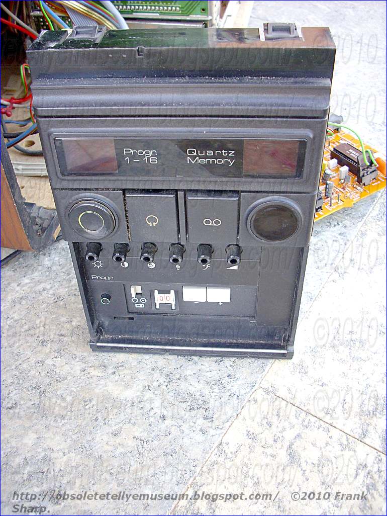
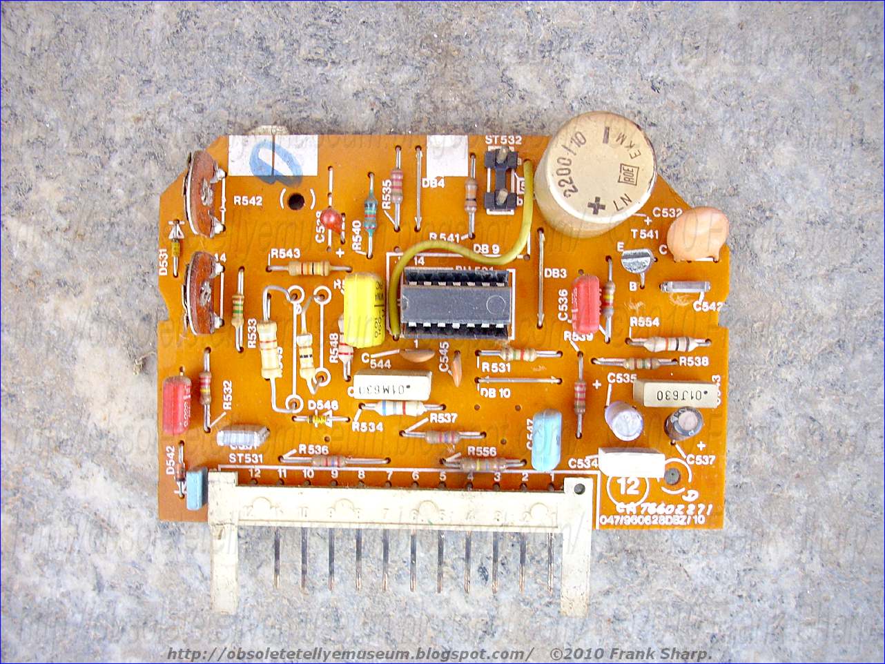
TELEFUNKEN PALCOLOR 8848J QUARTZ MEMORY / TELEFUNKEN CHASSIS 712A DPS2 Drive circuit for an infrared remote control transmitter:
An infrared remote control transmitter includes at least one infrared light-emitting diode poled with respect to a point of reference potential so as to be conductive in response to voltages having the opposite polarity of a DC supply voltage and to be nonconductive in response to voltages having the same polarity as the DC supply voltage. A pus
 h-pull amplifier is responsive to a pulse signal encoded to represent a remote control message to selectively couple the DC supply voltage or the reference potential to a capacitor coupled in series between the push-pull amplifier and the light-emitting diode. The capacitor is charged and discharged and an alternating drive voltage for the light-emitting diode having portions with polarities both the same as and opposite to the polarity of the DC supply voltage is generated. The push-pull amplifier is arranged so that when a component failure occurs, the portions of the alternating drive voltage having the polarity opposite to the polarity of the DC supply voltage are at least inhibited to prevent the continuous (i.e., DC) emission of infrared radiation.
 1. In an infrared remote control transmitter for controlling a television system, apparatus comprising:
a reference circuit point for receiving a reference potential;
a supply circuit point for receiving a DC supply voltage;
a battery connected with a predetermined polarity connected between said supply and reference circuit points;
at least one light-emitting diode for emitting infrared radiation when rendered conductive, said light emitting diode having a cathode and an anode, one of said cathode and anode being connected to said reference circuit point, said light-emitting diode being poled with respect to said reference circuit point so as to be conductive in response to the application of a voltage to the other one of said cathode and anode having the opposite polarity to said battery with respect to said reference circuit point and non-conductive in response to the application of a voltage to said other one of said cathode and anode having the same polarity as said battery with respect to said reference circuit point;
a source cir
a drive circuit point;
a capacitor directly connected between said drive circuit point and said other one of said cathode and anode;
a diode directly connected between said other one of said cathode and anode and said reference circuit point and poled in the opposite sense to said light-emitting diode with respect to said reference circuit point;
push-pull amplifier means for developing a drive voltage at said drive point including first and second bipolar transistors of opposite conduction types, each of said transistors having a collector-emitter path and a base electrode for controlling the conduction of said collector-emitter path, said collector-emitter path of said first transistor being directly connected between said supply circuit point and said drive circuit point, said collector-emitter path of said second transistor being connected between said drive circuit point and said reference point; and
input means coupled between said source circuit point and said bases of said first and second transistors for rendering said collector-emitter path of said first transistor conductive and said collector-emitter path of said second transistor non-conductive in response to a first portion of said pulses of said input signal and for rendering said collector-emitter path of said second transistor conductive and said collector-emitter path of said first transistor non-conductive in response to a second portion of said pulses of said input signal.
2. The apparatus recited in claim 1 wherein:
three light-emitting diodes poled in the same direction are connected in series between said capacitor means and said reference circuit point.
3. The apparatus recited in claim 1 wherein:
a second capacitor is directly connected between said drive point and said other one of said cathode and anode in parallel with said first mentioned capacitor directly connected between said drive point and said other one of said cathode and anode.4. The apparatus recited in claim 1 wherein:
said input means includes a first capacitor connected between said source circuit point and said base of said first transistor; first means connected between said supply circuit point and said base of said first transistor for discharging said first capacitor; a second capacitor connected between said source circuit point and said base of said second transistor; and second means connected between said base of said second transistor and said reference circuit point for discharging said second capacitor.
5. The apparatus recited in claim 4 wherein:
said first means includes a further diode poled to be conductive when said collector-emitter path of said first transistor is non-conductive and non-conductive when said collector-emitter path of said first transistor is conductive; and
said second means includes a still further diode poled to be conductive when said collector-emitter path of said second transistor is non-con
ductive and non-conductive when said collector-emitter path of said second transistor is conductive.6. In an infrared remote control transmitter for controlling a television system, apparatus comprising:
a reference circuit point for receiving a reference potential;
a supply circuit point for receiving a DC supply voltage;
a battery connected with a predetermined polarity connected between said supply and reference circuit points;
three light-emitting diodes which emit infrared radiation when rendered conductive directly connected in series between a voltage application circuit point and said reference circuit point, all of said light-emitting diodes being poled with respect to said reference circuit point so as to be conductive in response to the application of a voltage to said voltage application circuit point having the opposite polarity to said battery with respect to said reference circuit point and non-conductive in response to the application of a voltage to said voltage application circuit point having the same polarity as said battery with respect to said reference circuit point;
a source circuit point for receiving an input signal having pulses encoded to represent information for controlling a predetermined function of said television receiver;
a drive circuit point;
a first capacitor directly connected between said drive circuit point and said voltage application circuit point;
a second capacitor directly connected between said drive circuit point and said voltage application circuit point;
a diode directly connected between said voltage application circuit point and said reference circuit point and poled in the opposite sense to said light-emitting diode with respect to said reference circuit point;

input means coupled between said source circuit point and said bases of said first and second transistors for rendering said collector-emitter path of said first transistor conductive and said collector-emitter path of said second transistor non-conductive in response to a first portion of said pulses of said input signal and for rendering said collector-emitter path of said second transistor conductive and said collector-emitter path of said first transistor non-conductive in response to a second portion of said pulses of said input signal.
Description:
BACKGROUND OF THE PRESENT INVENTION
Th e present invention relates to drive circuits for infrared remote control transmitters.
Infrared remote control systems for television receivers and the like are known. The chief advantage of infrared remote control systems in comparison to ultrasonic remote control systems is that they are less susceptible to erroneously-generated interference signals. Unfortunately, the human eye may be harmed under conditions of prolonged, continuous and direct exposure to infrared radiation.
In order to reduce the possibility of harm to the eyes of users, infrared remote control systems utilize special pulse codes which minimize the duration of infrared radiation during the transmission of remote controlled messages. However, since in conventional drive circuits for infrared remote control transmitters the infrared light source, e.g., a light-emitting diode or diodes, is typically included in a direct current path from a supply voltage, infrared radiation may be continuously emitted should there be a component failure in the remote control transmitter. Therefore, there is a requirement for drive circuits for use in infrared remote control transmitters in which component failures do not result in the continuous emission of infrared radiation. The present invention concerns such a "fail-safe" drive circuit.
SUMMARY OF THE PRESENT INVENTION
In a remote control transmitter, at least one infrared light-emitting diode is coupled to a point of reference potential and poled so as to be substantially nonconductive in response to voltages having the same polarity as a DC supply voltage for the transmitter and substantially conductive in response to voltages having the polarity opposite to the polarity of the DC supply voltage. Driver means responsive to an input signal is coupled between the source of the DC supply voltage and the light-emitting diode. The driver means normally generates an alternating drive voltage for the light-emitting diode having portions with polarities both the same as and opposite to the polarity of the DC supply voltage. The driver means is arranged so that the portions of the drive signal having the polarity opposite to that of the DC supply voltage are at least inhibited when a component failure occurs.
BRIEF DESCRIPTION OF THE DRAWING
The sole FIGURE of the drawing shows, partially in block diagram form and partially in schematic diagram form, an infrared remote control system constructed in accordance with the present invention as it may be employed in a television receiver arrangement.
DETAILED DESCRIPTION OF THE DRAWING
A tele vision receiver 1 includes an antenna 3, a tuner 5, an IF signal processing unit 7, a picture signal processing unit 9, a sound signal processing unit 11, a picture tube 13 and a speaker 15 arranged in a conventional fashion to produce visual and audio responses. A power supply 17 is selectively energized to generate DC supply voltages for the portions of the receiver so far described from the AC line voltage in response to an ON/OFF control signal generated by a remote control receiver 19. Receiver 1 also includes a standby power supply 20 which continuously couples a DC supply voltage to remote control receiver 19 so that it is ready to accept messages from a remote control transmitter 21.
Remote control receiver 19 includes a photosensitive diode 23. The conduction of photo diode 23 is controlled in response to encoded optical signals having frequencies in the infrared range generated by remote control transmitter 21. A detector 25 senses the changes in the conduction of diode 23 and generates electrical signals corresponding to the encoded optical signals. The electrical signals are decoded by a decoder 27 to generate the ON/OFF control signal for tuning receiver 1 on and off, a CHANNEL SELECTION control signal for controlling the frequency to which a tuner 5 is tuned, and a VOLUME control signal for controlling the sound level of receiver 1.
Remote control transmitter 21 includes a ke yboard 29 including push buttons (not shown) by which a user may control the various receiver functions enumerated above. When a push button is depressed a corresponding electrical signal is generated by keyboard 29. A pulse encoder 31 is responsive to these electrical signals to generate respective coded pulse signals. The coded pulse signals are processed by a driver 33 to cause infrared light-emitting diodes 35, 37 and 39 to generate corresponding optical signals in the infrared frequency range.
Various codes for infrared remote control systems and encoders and decoders for these codes are known. For example, encoder 31 and decoder 27 may comprise S2600 and S2601 integrated circuits manufactured by American Microsystems, Inc. of Santa Clara, Calif.
The exact nature of the codes is not directly germane to the present invention. However, it is desirable for the reasons of safety discussed earlier that the code formats are arranged so that the duration of infrared radiation during a transmission is minimized. Since the pulses of the pulse signals generated by pulse encoder 31 correspond to the intervals of infrared radiation, this may be accomplished by causing the electrical pulse signals generated by encoder 31 to have a relatively low duty cycle, e.g., less than 20 percent. In addition, for safety reasons, it is desirable that light-emitting diodes 35, 37 and 39 be physically separated on transmitter 21 from one another by a distance selected so that the power of the infrared radiation they generate is distributed rather than concentrated in a relatively small area.
While these safety precautions to some extent minimize the danger to users, they do not account for component failures which may cause the continuous, i.e., DC, emission of infrared radiation. Unfortunately, the human eye may be injured when directly exposed to continuous infrared radiation for prolonged periods. While such situations are extremely rare, since they would involve not only a component failure but the misuse of the transmitter, they may occur under extraordinary circumstances. For example, a curious child may point an infrared transmitter with a failed component directly into his eye.
Drive circuit 33 is arranged to prevent the continuous emission of infrared radiation under any for eseeable component failure mode. Driver 33 includes a push-pull amplifier 41 comprising a PNP transistor 43 and an NPN transistor 45 having their collector-emitter junctions coupled in series between a battery 47 and signal ground. Battery 47 is the source of DC supply voltage for transmitter 21. The output of pulse encoder 31 is coupled to the bases of transistors 43 and 45 through capacitors 49 and 51, respectively. Diodes 53 and 55 are coupled in shunt with the base-emitter junctions of transistors 43 and 45, respectively. The junction of the collectors of transistors 43 and 45 is coupled through parallel connected capacitors 57 and 58 to the cathode of light-emitting diode 35. Light-emitting diodes 35, 37 and 39 are connected in series with the same polarity between capacitors 57 and 58 and signal ground. The polarity of light-emitting diodes 35, 37 and 39 is selected so that they are rendered nonconductive in response to the application of voltages to the cathode of light-emitting diode 35 having the same polarity (i.e., positive) with respect to signal ground as the DC supply voltage provided by battery 47 and only rendered conductive in response to the application of voltages having the opposite polarity (i.e., negative) with respect to signal ground to the DC supply voltage. A diode 59 is connected in shunt with series connected light-emitting diodes 35, 37 and 39 and poled in the opposite direction.
In operation, pulse encoder 31 generates a pulse signal encoded as described above. The pulse signal includes positive-going pulses. In response to the leading edges of the positive-going pulses, transistor 45 is rendered conductive. In response to the trailing edges of the positive-going pulses, transistor 43 is rendered conductive. Diodes 53 and 55 serve as discharge paths for capacitors 49 and 51 during the intervals when transistors 43 and 45, respectively, are nonconductive. Diodes 53 and 55 also clamp the voltage at the bases of transistors 43 and 45 close to the battery voltage and the voltage at signal ground, respectively, in order to protect the base-emitter junctions of transistors 43 and 45 from reverse breakdown failure voltages. Desirably, capacitors 49 and 51 have relatively small values so that capacitors 49 and 51 are charged and discharged in response to each pulse. As a result, transistors 43 and 45 are alternately rendered conductive and nonconductive in response to each pulse of the pulse signal.
When transistor 43 is conductive (and transistor 45 is nonconductive) capacitors 57 and 58 are charged from battery 47. When transistor 45 is conductive (and transistor 43 is nonconductive) capacitors 57 and 58 are discharged to signal ground. As a result, an alternating drive voltage, i.e., one having polarity excursions above and below the potential at signal ground, are generated at the cathode of light-emitting diode 35. Light-emitting diodes are conductive in response to the negative portions of the drive voltage and are nonconductive in response to the positive portions of the drive voltage. Diodes 35, 37 and 39 only emit infrared radiation when they are conductive. Therefore, infrared radiation is only emitted by transmitter 21 when the drive voltage has a polarity (i.e., negative opposite to the polarity of the DC supply voltage.
Desirably, the capacitance of the combination of capacitors 57 and 58 is relatively large, e.g., 1 microfarad, so that sufficient drive current is provided to light-emitting diodes 35, 37 and 39 to cause them to emit infrared radiation. For the same reason, two capacitors rather than one are used, since the effective series resistance associated with the parallel combination is smaller than the series resistance of a single capacitor.
In the event that there is a component failure within drive circuit 33, drive voltage developed at the cathode of light-emitting diode 35 will be reduced and, in most cases, substantially inhibited. Under these conditions, since the amplitude of the negative portions of the drive signal will at least have a lower than normal amplitude, the infrared radiation will have a lower than normal energy.
 Briefly, any failure of a component within driver 33 causing the component to open or short, substantially prevents the development of an alternating drive signal at the cathode of light-emitting diode 35. Since diodes 35, 37 and 39 are rendered conductive only in response to negative-going voltages, no infrared radiation is generated. Any component failure between the extremes of an open or short causes a reduction in the amplitude of the alternating drive signal. By way of example, consider the following failure modes. If either transistor 43 or 45 fails, e.g., by shorting from collector to emitter, capacitors 57 and 58 will be either permanently charged or discharged, thereby preventing the development of an alternating drive signal. If one of capacitors 57 and 58 shorts, only positive-going voltages are developed at the cathode of light-emitting diode 35. If the collector to emitter junction of transistor 43 and one of capacitors 57 and 58 short, a DC signal is coupled to the cathode of light-emitting diode 35, thereby rendering diode 59 conductive and preventing light-emitting diodes 35, 37 and 39 from being rendered conductive. If diode 59 opens, capacitors 57 and 58 will not be charged thereby preventing the development of an alternating voltage at the cathode of diode 35. If diode 59 fails so as to lose its unidirectional conductive characteristics, i.e., in essence becomes a passive element, an alternating drive signal will be developed but it will have a lower than normal amplitude. Furthermore, failures in pulse encoder 31 causing generation of a DC signal rather than a pulse signal will also cause the loss of an alternating drive signal.
Driver circuit 33 may be modified in some respects without causing the loss of its "fail-safe" nature. For example, any or all of diodes 53, 55 and 59 may be replaced with resistors. While this modification causes a reduction in efficiency of the normal operation of drive circuit 33, it does not alter its "fail-safe" nature. These and other modifications are intended to be within the scope of the present invention as set forth in the following claims.
TELEFUNKEN CHASSIS 712A Tuning circuit arrangement
A tuning circuit arrangement comprises one or more tuned circuits whose frequency range is tuned by tuning diodes, means being provided for varying the tuning voltage of the tuning diodes to provide exclusive variation of the tuned circuit capacitance of the tuned circuit.
 1. A circuit for adjusting a tuning circuit, the tuning circuit including at least one resonant circuit composed of a variable inductance and a variable capacitance constituted by at least one voltage-variable tuning diode, one side of the resonant circuit being connected to a point at circuit ground potential and adjustment of the resonant circuit being effected by changing the resonant circuit inductance and the resonant circuit capacitance, with changing of the resonant circuit capacitance being effected exclusively by varying the tuning voltage of the tuning diode, the tuning circuit further including a source of a variable tuning potential which is variable over a range between maximum and minimum extreme values, each extreme value being different from the circuit ground potential, and said circuit for adjusting comprising at least one adjustment potentiometer connected between a point of said source providing the variable tuning potential and a point of said source permanently providing one of said extreme values, said potentiometer having an adjustable tap connected to provide the tuning voltage for said tuning diode. 2. An arrangement as defined in claim 1 wherein said tuning circuit includes a plurality of said resonant circuits and said circuit for adjusting comprises a plurality of said potentiometers connected together in parallel and each having a respective adjustable tap connected to provide the tuning voltage for at least one respective tuning diode. 3. An arrangement as defined in claim 1 wherein said source comprises a tuning potentiometer connected to have a respective one of the extreme values of the tuning potential at each of its ends and having an adjustable tap providing the variable tuning potential, and said adjustment potentiometer is connected between one end and said movable tap of said tuning potentiometer. 4. An arrangement as defined in claim 1 wherein said tuning circuit includes at least two of said resonant circuits and said adjustable tap of said adjustment potentiometer is connected to provide the tuning voltage for said at least two resonant circuits. 5. An arrangement as defined in claim 4 wherein said resonant circuits have respectively different relative frequency variations.
Th
 e present invention relates to drive circuits for infrared remote control transmitters.
Infrared remote control systems for television receivers and the like are known. The chief advantage of infrared remote control systems in comparison to ultrasonic remote control systems is that they are less susceptible to erroneously-generated interference signals. Unfortunately, the human eye may be harmed under conditions of prolonged, continuous and direct exposure to infrared radiation.
In order to reduce the possibility of harm to the eyes of users, infrared remote control systems utilize special pulse codes which minimize the duration of infrared radiation during the transmission of remote controlled messages. However, since in conventional drive circuits for infrared remote control transmitters the infrared light source, e.g., a light-emitting diode or diodes, is typically included in a direct current path from a supply voltage, infrared radiation may be continuously emitted should there be a component failure in the remote control transmitter. Therefore, there is a requirement for drive circuits for use in infrared remote control transmitters in which component failures do not result in the continuous emission of infrared radiation. The present invention concerns such a "fail-safe" drive circuit.
SUMMARY OF THE PRESENT INVENTION
In a remote control transmitter, at least one infrared light-emitting diode is coupled to a point of reference potential and poled so as to be substantially nonconductive in response to voltages having the same polarity as a DC supply voltage for the transmitter and substantially conductive in response to voltages having the polarity opposite to the polarity of the DC supply voltage. Driver means responsive to an input signal is coupled between the source of the DC supply voltage and the light-emitting diode. The driver means normally generates an alternating drive voltage for the light-emitting diode having portions with polarities both the same as and opposite to the polarity of the DC supply voltage. The driver means is arranged so that the portions of the drive signal having the polarity opposite to that of the DC supply voltage are at least inhibited when a component failure occurs.
BRIEF DESCRIPTION OF THE DRAWING
The sole FIGURE of the drawing shows, partially in block diagram form and partially in schematic diagram form, an infrared remote control system constructed in accordance with the present invention as it may be employed in a television receiver arrangement.
DETAILED DESCRIPTION OF THE DRAWING
A tele
vision receiver 1 includes an antenna 3, a tuner 5, an IF signal processing unit 7, a picture signal processing unit 9, a sound signal processing unit 11, a picture tube 13 and a speaker 15 arranged in a conventional fashion to produce visual and audio responses. A power supply 17 is selectively energized to generate DC supply voltages for the portions of the receiver so far described from the AC line voltage in response to an ON/OFF control signal generated by a remote control receiver 19. Receiver 1 also includes a standby power supply 20 which continuously couples a DC supply voltage to remote control receiver 19 so that it is ready to accept messages from a remote control transmitter 21.Remote control receiver 19 includes a photosensitive diode 23. The conduction of photo diode 23 is controlled in response to encoded optical signals having frequencies in the infrared range generated by remote control transmitter 21. A detector 25 senses the changes in the conduction of diode 23 and generates electrical signals corresponding to the encoded optical signals. The electrical signals are decoded by a decoder 27 to generate the ON/OFF control signal for tuning receiver 1 on and off, a CHANNEL SELECTION control signal for controlling the frequency to which a tuner 5 is tuned, and a VOLUME control signal for controlling the sound level of receiver 1.
Remote control transmitter 21 includes a ke
yboard 29 including push buttons (not shown) by which a user may control the various receiver functions enumerated above. When a push button is depressed a corresponding electrical signal is generated by keyboard 29. A pulse encoder 31 is responsive to these electrical signals to generate respective coded pulse signals. The coded pulse signals are processed by a driver 33 to cause infrared light-emitting diodes 35, 37 and 39 to generate corresponding optical signals in the infrared frequency range.Various codes for infrared remote control systems and encoders and decoders for these codes are known. For example, encoder 31 and decoder 27 may comprise S2600 and S2601 integrated circuits manufactured by American Microsystems, Inc. of Santa Clara, Calif.
The exact nature of the codes is not directly germane to the present invention. However, it is desirable for the reasons of safety discussed earlier that the code formats are arranged so that the duration of infrared radiation during a transmission is minimized. Since the pulses of the pulse signals generated by pulse encoder 31 correspond to the intervals of infrared radiation, this may be accomplished by causing the electrical pulse signals generated by encoder 31 to have a relatively low duty cycle, e.g., less than 20 percent. In addition, for safety reasons, it is desirable that light-emitting diodes 35, 37 and 39 be physically separated on transmitter 21 from one another by a distance selected so that the power of the infrared radiation they generate is distributed rather than concentrated in a relatively small area.
While these safety precautions to some extent minimize the danger to users, they do not account for component failures which may cause the continuous, i.e., DC, emission of infrared radiation. Unfortunately, the human eye may be injured when directly exposed to continuous infrared radiation for prolonged periods. While such situations are extremely rare, since they would involve not only a component failure but the misuse of the transmitter, they may occur under extraordinary circumstances. For example, a curious child may point an infrared transmitter with a failed component directly into his eye.
Drive circuit 33 is arranged to prevent the continuous emission of infrared radiation under any for
eseeable component failure mode. Driver 33 includes a push-pull amplifier 41 comprising a PNP transistor 43 and an NPN transistor 45 having their collector-emitter junctions coupled in series between a battery 47 and signal ground. Battery 47 is the source of DC supply voltage for transmitter 21. The output of pulse encoder 31 is coupled to the bases of transistors 43 and 45 through capacitors 49 and 51, respectively. Diodes 53 and 55 are coupled in shunt with the base-emitter junctions of transistors 43 and 45, respectively. The junction of the collectors of transistors 43 and 45 is coupled through parallel connected capacitors 57 and 58 to the cathode of light-emitting diode 35. Light-emitting diodes 35, 37 and 39 are connected in series with the same polarity between capacitors 57 and 58 and signal ground. The polarity of light-emitting diodes 35, 37 and 39 is selected so that they are rendered nonconductive in response to the application of voltages to the cathode of light-emitting diode 35 having the same polarity (i.e., positive) with respect to signal ground as the DC supply voltage provided by battery 47 and only rendered conductive in response to the application of voltages having the opposite polarity (i.e., negative) with respect to signal ground to the DC supply voltage. A diode 59 is connected in shunt with series connected light-emitting diodes 35, 37 and 39 and poled in the opposite direction.In operation, pulse encoder 31 generates a pulse signal encoded as described above. The pulse signal includes positive-going pulses. In response to the leading edges of the positive-going pulses, transistor 45 is rendered conductive. In response to the trailing edges of the positive-going pulses, transistor 43 is rendered conductive. Diodes 53 and 55 serve as discharge paths for capacitors 49 and 51 during the intervals when transistors 43 and 45, respectively, are nonconductive. Diodes 53 and 55 also clamp the voltage at the bases of transistors 43 and 45 close to the battery voltage and the voltage at signal ground, respectively, in order to protect the base-emitter junctions of transistors 43 and 45 from reverse breakdown failure voltages. Desirably, capacitors 49 and 51 have relatively small values so that capacitors 49 and 51 are charged and discharged in response to each pulse. As a result, transistors 43 and 45 are alternately rendered conductive and nonconductive in response to each pulse of the pulse signal.
When transistor 43 is conductive (and transistor 45 is nonconductive) capacitors 57 and 58 are charged from battery 47. When transistor 45 is conductive (and transistor 43 is nonconductive) capacitors 57 and 58 are discharged to signal ground. As a result, an alternating drive voltage, i.e., one having polarity excursions above and below the potential at signal ground, are generated at the cathode of light-emitting diode 35. Light-emitting diodes are conductive in response to the negative portions of the drive voltage and are nonconductive in response to the positive portions of the drive voltage. Diodes 35, 37 and 39 only emit infrared radiation when they are conductive. Therefore, infrared radiation is only emitted by transmitter 21 when the drive voltage has a polarity (i.e., negative opposite to the polarity of the DC supply voltage.
Desirably, the capacitance of the combination of capacitors 57 and 58 is relatively large, e.g., 1 microfarad, so that sufficient drive current is provided to light-emitting diodes 35, 37 and 39 to cause them to emit infrared radiation. For the same reason, two capacitors rather than one are used, since the effective series resistance associated with the parallel combination is smaller than the series resistance of a single capacitor.
In the event that there is a component failure within drive circuit 33, drive voltage developed at the cathode of light-emitting diode 35 will be reduced and, in most cases, substantially inhibited. Under these conditions, since the amplitude of the negative portions of the drive signal will at least have a lower than normal amplitude, the infrared radiation will have a lower than normal energy.
positive-going voltages are developed at the cathode of light-emitting diode 35. If the collector to emitter junction of transistor 43 and one of capacitors 57 and 58 short, a DC signal is coupled to the cathode of light-emitting diode 35, thereby rendering diode 59 conductive and preventing light-emitting diodes 35, 37 and 39 from being rendered conductive. If diode 59 opens, capacitors 57 and 58 will not be charged thereby preventing the development of an alternating voltage at the cathode of diode 35. If diode 59 fails so as to lose its unidirectional conductive characteristics, i.e., in essence becomes a passive element, an alternating drive signal will be developed but it will have a lower than normal amplitude. Furthermore, failures in pulse encoder 31 causing generation of a DC signal rather than a pulse signal will also cause the loss of an alternating drive signal.Driver circuit 33 may be modified in some respects without causing the loss of its "fail-safe" nature. For example, any or all of diodes 53, 55 and 59 may be replaced with resistors. While this modification causes a reduction in efficiency of the normal operation of drive circuit 33, it does not alter its "fail-safe" nature. These and other modifications are intended to be within the scope of the present invention as set forth in the following claims.
TELEFUNKEN CHASSIS 712A Tuning circuit arrangement
A tuning circuit arrangement comprises one or more tuned circuits whose frequency range is tuned by tuning diodes, means being provided for varying the tuning voltage of the tuning diodes to provide exclusive variation of the tuned circuit capacitance of the tuned circuit.
1. A circuit for adjusting a tuning circuit, the tuning circuit including at least one resonant circuit composed of a variable inductance and a variable capacitance constituted by at least one voltage-variable tuning diode, one side of the resonant circuit being connected to a point at circuit ground potential and adjustment of the resonant circuit being effected by changing the resonant circuit inductance and the resonant circuit capacitance, with changing of the resonant circuit capacitance being effected exclusively by varying the tuning voltage of the tuning diode, the tuning circuit further including a source of a variable tuning potential which is variable over a range between maximum and minimum extreme values, each extreme value being different from the circuit ground potential, and said circuit for adjusting comprising at least one adjustment potentiometer connected between a point of said source providing the variable tuning potential and a point of said source permanently providing one of said extreme values, said potentiometer having an adjustable tap connected to provide the tuning voltage for said tuning diode. 2. An arrangement as defined in claim 1 wherein said tuning circuit includes a plurality of said resonant circuits and said circuit for adjusting comprises a plurality of said potentiometers connected together in parallel and each having a respective adjustable tap connected to provide the tuning voltage for at least one respective tuning diode. 3. An arrangement as defined in claim 1 wherein said source comprises a tuning potentiometer connected to have a respective one of the extreme values of the tuning potential at each of its ends and having an adjustable tap providing the variable tuning potential, and said adjustment potentiometer is connected between one end and said movable tap of said tuning potentiometer. 4. An arrangement as defined in claim 1 wherein said tuning circuit includes at least two of said resonant circuits and said adjustable tap of said adjustment potentiometer is connected to provide the tuning voltage for said at least two resonant circuits. 5. An arrangement as defined in claim 4 wherein said resonant circuits have respectively different relative frequency variations.
Description:
BACKGROUND OF THE INVENTION
 The invention relates to a tuning circuit arrangement comprising one or more tuning circuits in which tuning diodes are provided for tuning of the frequency range. In such an arrangement, the adjustment of the tuned circuit takes place, for example, by changing the tuned circuit inductance and the tuned circuit capacitance.
As is known, tuning circuits have the object of tuning the resonant circuits of selective amplifiers and/or oscillators to a given resonant frequency. In a known tuning circuit, the adjustment to synchronous operation in each circuit takes place via a tuning coil and a particular trimmer capacitor. In the known tuning circuit arrangement a multiply repeated adjustment of the inductance and the capacitance is required for adjustment to synchronous operation, because the setting of the trimmer capacitors again changes the resonant frequency of the frequency previously set inductively.
SUMMARY OF THE INVENTION
Itis an object of the invention to provide a tuning circuit arrangement with simplified adjustment.
According to a first aspect of the invention, there is provided a tuning circuit arrangement comprising one or more tuned circuits, tuning diodes in said tuned circuits for tuning the frequency range of said tuned circuits and means for varying the tuning voltage of said tuning diodes for providing exclusive variation of the tuned circuit capacitance of said tuned circuit.
According to a second aspect of the invention, there is provided a tuning circuit arrangement comprising one or more tuning circuits, in which tuning diodes are provided for the purpose of tuning the frequency range and in which the tuned circuit adjustment takes place by changing the tuned circuit inductance and the tuned circuit capacitance, characterized in that the adjustment in capacitance takes place exclusively by varying the tuning voltage for the tuning diode(s).
BRIEF DESCRIPTION OF THE DRAWINGS
The invention will now be described in greater detail, by way of example, with reference to the drawings in which:
FIG. 1 is a circuit diagram showing a first form of circuit arrangement in accordance with the invention as applied to two resonant circuits;
FIG. 2 is a circuit diagram similar to FIG. 1 but showing the arrangement applied to n resonant circuits;
FIG. 3 is a circuit diagram similar to FIG. 1 but showing the arrangement with a different form of adjustment;
FIG. 4 is a circuit diagram similar to FIG. 2 in which the arrangement of FIG. 3 is applied to n resonant circuits;
FIG. 5 is a circuit diagram showing a part of the arrangement showing a different form of adjusting circuitry;
FIG. 6 is a circuit diagram similar to FIG. 5 but showing a still further form of adjusting circuitry;
FIG. 7 is a block diagram of part of the arrangement provided with temperature compensation and,
FIG. 8 is a block diagram similar to FIG. 7 but including a decoupling circuit.
DESCRIPTION OF THE PREFERRED EMBODIMENTS
In a tuning circuit arrangement of the type mentioned at the beginning it is proposed in accord ance with the invention and in order to solve the object that the adjustment in capacitance should take place exclusively by variation of the tuning voltage for the tuning diode(s).
The essence of the invention on the one hand consists in that special trimmer capacitors for achieving an adjustment in capacitance are omitted and that the adjustment in capacitance takes place exclusively by variations of the tuning voltage for the tuning diode(s) which is in contrast to the known method, and does not take place by means of trimmer capacitors. On the other hand, the invention does not require any repetitive adjustment of the tuned circuits of the tuning circuits.
The tuning circuit arrangement in accordance with the invention makes it possible to reduce considerably the required maximum tuning voltage. With the tuning circuit arrangement in accordance with the invention it is possible to operate with small tuning voltages even when using tuning diodes having abrupt pn junction. The sought after simplification of the adjustment can be achieved by means of the fact that the capacitative adjustment does not influence the previously operated adjustment in inductance.
In the tuning circuit arrangement according to the invention potentiometers, for example, are provided in order to adjust the capacitance. There is the possibility of using the same adjusting means for adjusting the capacitance of two or more tuned circuits. Similarly, the same adjustment means may serve to adjust the capacitance of several tuned circuits having varying relative frequency variation.
In accordance with a further refinement of the invention a circuit arrangement for producing minimum and maximum tuning potentials is provided which is constructed so that the potentials produced by it have such a temperature dependence that the effect of temperature on the tuning circuit is compensated.
It is advisable to connect a decoupling circuit between the means for adjusting capacitance and the 6 tuning potentiometers, the decoupling circuit reducing the electrical load on the tuning potentiometer through the adjustment means. In accordance with an embodiment of the invention, precautions are taken to ensure that one of the two potentials applied to an adjustment potentiometer, does not change during adjustment.
The adjustment potentiometer or potentiometers are connected for example between a point in the circuit at which the variable tuning potential is available and a point in the circuit at which the minimum tuning potential is available. There is also the possibility of connecting the adjustment potentiometer or potentiometers between a point in the circuit at which the variable tuning potential is available and a point in the circuit at which the maximum tuning potential is available.
Referring now to the drawings, FIG. 1 shows an electronic tuning circuit in accordance with the inv ention which operates with tuning diodes. The tuning circuit of FIG. 1, which is for example a component of a VHF tuner, consists of two variable-frequency resonant circuits and in fact an oscillator circuit 1 and a resonant circuit 2 for selecting the input signal. The oscillator circuit comprises an inductance 3 and a tuning diode 4, which is a double diode in this embodiment. The resonant circuit 2 comprises an inductance 5 and a tuning diode 6, which in this embodiment is also a double diode. As may be seen from FIG. 1, neither of the two resonant circuits 1 and 2 has a trimmer capacitor. Of course, parallel to the resonant circuits there are unavoidable circuit capacitances 7 and 8 which are shown in broken lines.
The two resonant circuits 1 and 2 must be adjusted to achieve synchronous operation. In accordance with the invention the adjustment potentiometers 9 and 10 are provided for this purpose. The adjustment potentiometers 9 and 10 are connected in parallel with one another in the embodiment of FIG. 1. Two limiting potentials are required for the tuning circuit; in fact the largest potential U max at point 11 and the smallest potential U min at point 12. In the embodiment of FIG. 1 the two adjustment potentiometers 9 and 10 lie between the wiper contact 13 of the tuning potentiometer 14 and the point 12 having the potential U min . The tuning potentiometer 14 lies between the points 11 and 12, i.e. between the maximum potential U max and the minimum potential U min . The maximum tuning potential U max and the minimum tuning potential U min are in fact linked together, yet they are produced in a separate circuit arrangement. This is indicated symbolically in FIG. 1 by means of the two voltage sources 23 and 24. The minimum tuning potential U min is therefore not derived via a purely ohmic voltage divider from the maximum tuning potential U max .
In the tuning circuit of FIG. 1, in the case where the tuning potentiometer 14 is set to the minimum tuning voltage, the voltages taken from the adjustment potentiometers 9 and 10 are not influenced by the settings of the adjustment potentiometer. Therefore, if the wiper contact 13 of the tuning potentiometer 14 is located at the lowest position then no matter how the adjustment potentiometers 9 and 10 are rotated the adjustment voltages for the tuning diodes will not be influenced by this. This has the consequence that setting in the upper frequency range has no influence on the previously set lower frequency. The adjustment of the lower frequency is only dependent on the inductance adjustment of the inductances 3 and 5.
The tuning circuit of FIG. 2 is distinguished from the tuning circuit of FIG. 1 by the fact that instead of only two resonant circuits n resonant circuits are provided and, instead of only two adjustment potentiometers, m adjustment potentiometers are provided. m may be smaller than n if not merely one resonant circuit but more than one resonant circuit is adjusted by means of a single adjustment potentiometer.
FIG. 3 shows an embodiment of the invention in which in contrast to FIGS. 1 and 2 the adjustment potentiometers 9 and 10 lie between the wiper contact 13 of the tuning potentiometer 14 and point 11 having the potential U max . In this case, the adjustment in inductance takes place in the upper frequency and the adjustment in capacitance takes place in the lower frequency by means of the adjustment potentiometers 9 and 10.
The tuning circuit of FIG. 4 is distinguished from the tuning circuit of FIG. 3 by the fact that, instead of only two resonant circuits, again n resonant circuits are provided and instead of only two adjustment potentiometers m adjustment potentiometers are provided.
According to FIG. 5 the adjustment in capacitance is undertaken for the upper frequency by setting the maximum tuning potential. While in the tuning circuits of FIGS. 1 to 4 the adjustment of the individual tuned circuits is independent, in the arrangement of FIG. 5 the setting of the maximum tuning potential effects all tuned circuits. The setting of the maximum tuning potential takes place in the arrangement of FIG. 5 by means of the voltage source 20. The voltage supplying the tuning diodes may for example be taken from the wiper contact 13 of the tuning potentiometer 14, from a fixed voltage divider 21 or from the wiper contact of the adjustment potentiometer 9. Several adjustment potentiometers may be provided instead of only one adjustment potentiometer.
The arrangement of FIG. 6 is distinguished from the arrangement of FIG. 5 by the fact that the minimum tuning potential is made settable instead of the maximum tuning potential for the purpose of adjustment. Moreover, in the arrangement of FIG. 6, the network which comprises the voltage divider 21 and the adjustment potentiometer 9, is connected between the wiper contact 13 of the adjustment potentiometer 14 and the maximum tuning potential 11.
According to FIG. 7, the maximum and minimum tuning potential is produced by means of a circuit arrangement 15 which has the object of supplying such a temperature effect of the potential that the temperature effect of the tuning circuit is compensated by an appropriate temperature effect of the potentials.
The arrangement 16 of FIG. 8 also produces the minimum and maximum tuning potentials at the points 11 and 12 as well as the effective temperature on these potentials which is required for temperature compensation of the tuning circuit. In addition, the arrangement 16 contains a decoupling circuit which lies between the wiper contact 13 of the tuning potentiometer 14 and the adjustment potentiometers 9 and 10.
The tuning circuit dealt with in the embodiments is developed for positive tuning potentials. In a similar manner, the tuning circuits of the invention may also be designed for negative tuning potentials.
It will be understood that the above description of the present invention is susceptible to various modification changes and adaptations.
TELEFUNKEN PALCOLOR 8848J QUARTZ MEMORY CHASSIS 712A DPS2 TELEFUNKEN PLL SYNTHESIZER PLESSEY CHIPSET CT1112 CT1111 Digital phase control circuit including an auxiliary circuit:

This application describes a receiver in which channel selection is controlled by a frequency synthesizer a sweep of available channels is made by a channel selecting arrangement and this sweep is arranged to be stopped when a signal is received. When the sweeping is stopped a fine tuning arrangement takes control to respond to the frequency of the received signal and to compensate for any drift of that signal. A tuning circuit for a high frequency receiver in which the received frequency is determined by a voltage-controlled oscillator, the present tuning frequency is indicated by a counter connected to the oscillator and producing a representation of each digit of the decimal number identifying the current received frequency, representations of the digits of the number identifying the desired received frequency are fed in via a rotary switch , and the decimal number representations are compared in a comparator to produce a control voltage that brings the oscillator frequency to the desired value, and in which the comparator is capable of comparing only one digit of the number representations at a time and receives the digits of corresponding significance in sequence, starting with the most significant digit, and the rate at which the control voltage is varied is made inversely proportional to the number of changes in the direction of the inequality of the digits of one of the number representations being compared relative to the corresponding digits of the other number representation being compared.
1. In a tuning circuit for a high frequency receiver, which circuit includes a voltage controllable superheterodyne oscillator arranged to receive a control voltage and to produce an oscillation whose frequency is determined by the value of the control voltage and determines the broadcast frequency to which the receiver is tuned, a counter connected to sense the frequency of the oscillations being generated by the oscillator and to produce therefrom a count state in the form of representations of the digits of a first decimal number identifying the broadcast frequency to which the receiver is currently tuned, input means for generating representations of the digits of a second decimal number identifying the broadcast frequency to which it is desired to tune the receiver, and a comparison circuit for comparing the decimal number representations being produced by the counter and the input means in order to vary the control voltage in a direction to cau
 se those two number representations to coincide, the comparison circuit including a comparator capable of comparing the representations of one digit of each of two numbers and having two inputs connected, respectively, to the counter and to the input means, the comparator being arranged to receive, at one of its inputs, each digit representation produced by the counter, starting with the most significant digit, and, at the other of its inputs, simultaneously therewith each digit representation of corresponding significance generated by the input means, the comparator including a first output providing a signal when the digit representations at its inputs are identical, a second output providing a signal when the digit representation at its one input represents a value larger than that of the digit representation at its other input, and a third output providing a signal when the digit representation at its one input represents a value smaller than that of the digit representation at its other input, the improvement comprising: tuning voltage adjustment means connected to said comparator outputs and responsive to the number of sequences of termination of a signal at one of said second and third outputs and subsequent initiation of a signal at the other of said second and third outputs for varying the control voltage at a rate inversely proportional to such number of sequences.
2. An arrangement as defined in claim 1 wherein said adjustment means comprises a sequence counter connected for counting the number of such sequences and having its count state set to zero at the beginning of each tuning operation.
3. An arrangement as defined in claim 2 wherein said adjustment means further comprises a logic gate connected to the output of said sequence counter and having a number of outputs equal to a selected number of desired control voltage variation rates, said gate being arranged to provide a certain logic potential at one of its outputs in dependence on the count state of said sequence counter.
4. An arrangement as defined in claim 3 wherein said comparison circuit includes an amplifier arranged to provide an output signal which effects variation of the control voltage, and said adjustment means further comprise a plurality of resistors having respectively different resistance values and each connected between a respective output of said gate and said amplifier for causing the control voltage variation rate to have a value determined by the resistance value of that resistor whose associated gate output is providing the certain logic potential.
 5. An arrangement as defined in claim 4 wherein the comparison circuit further includes a capacitor connected to receive the output signal from said amplifier so that the voltage thereacross constitutes the control voltage, said amplifier being arranged for supplying said capacitor with a charging or discharging current proportional to the current flowing through that one of said resistors whose associated gate output is providing the certain logic potential.
6. An arrangement as defined in claim 4 wherein said amplifier is connected to said second and third comparator outputs for causing the direction of variation of the control voltage to be determined on the basis of which one of said second and third comparator outputs is providing a signal.
7. An arrangement as defined in claim 4 wherein said gate is arranged to cause its outputs to be blocked at a selected maximum count state of said sequence counter for preventing current flow through any of said resistors.
8. An arrangement as defined in claim 4 wherein said logic gate is arranged to have its outputs blocked when there is coincidence between all digits of the two numbers.
9. An arrangement as defined in claim 2 wherein said adjustment means comprises a programmable frequency divider connected to have its dividing ratio determined by the counter state of said sequence counter in a manner such that the dividing ratio increases with increasing counter state.
10. An arrangement as defined in claim 9 wherein said adjustment means further comprises means for producing square wave oscillations of a constant frequency connected to feed such oscillations to said divider.
11. An arrangement as defined in claim 10 wherein said adjustment means comprises a digital-analog converter connected to the output of said divider and providing an output voltage whose value determines the magnitude of the rate of variation of the control voltage.
The present invention relates to a tuning circuit for a high frequency receiver having a superheterodyne oscillator whose frequency can be varied by means of a tuning voltage in order to tune the receiver to a desired station.
In such circuits, the tuning voltage, which is a direct voltage, is generated by a comparison circuit which effects a comparison between two numbers. The first number identifies the counter state of a counting device which periodically counts the oscillations of the superheterodyne oscillator on the basis of the intermediate frequency. This number thus constitutes the received frequency, or possibly the received channel or station. The second number is fed to the comparison circuit via an input keyboard provided with a series-connected coder and identifies the desired channel or station to which the receiver is to be tuned. The comparison circuit has three outputs, one output for the comparison result "equality" and one each for the two non-equality results "greater" and "less".
In the circuit disclosed in U.S. application Ser. No. 708,754, filed by the present applicant and Dieter Rottmann and Stephan Wuttke on July 26, 1976, the comparison is effected by a multiplex operation and the comparison circuit is composed of only a single comparator which can effect a comparison with respect to only one digit, or level of significance, of the numbers at a time. This comparator receives, in succession, the representations of the digits of the two numbers to be compared, beginning with the most significant digit.
If in the described tuning circuit the two numbers are unequal, the tuning circuit, and thus the frequency of the superheterodyne oscillator, is changed until the frequency identified by the number fed in has been attained. The rate at which the tuning voltage changes is relatively great if the two numbers to be compared differ from one another in all digit positions. The rate of change becomes less as more digits of the two numbers, beginning with the most significant digit, become equal. When all digits are equal, the frequency will no longer be changed. The tuning rate thus decreases as more digits become identical, this result being a function of the evaluation circuit provided in the above-cited application. The successive rates there are proportional to 1/2 . . . 1/n, where n = number of digit positions, e.g. 5. It has been found that this tuning process takes a relatively long time, which many operators consider to be a drawback.
SUMMARY OF THE INVENTION
It is therefore an object of the present invention to shorten the time required for the tuning process.
These and other objects are achieved, in a tuning circuit for a high frequency receiver, which circuit includes a voltage controllable superheterodyne oscillator arranged to receive a control voltage and to produce an oscillation whose frequency is determined by the value of the control voltage and determines the broadcast frequency to which the receiver is tuned, a counter connected to sense the frequency of the oscillations being generated by the oscillator and to produce therefrom a count state in the form of representations of the digits of a first decimal number identifying the broadcast frequency to which the receiver is currently tuned, input means for generating representations of the digits of a second decimal number identifying the broadcast frequency to which it is desired to tune the receiver, and a comparison circuit for comparing the decimal number representations being produced by the counter and the input means in order to vary the control voltage in a direction to cause those two number representations to coincide, the comparison circuit including a comparator capable of comparing the representations of one digit of each of two numbers and having two inputs connected, respectively, to the counter and to the input means, the comparator being arranged to receive, at one of its inputs, each digit representation produced by the counter, starting with the most significant digit, and, at the other of its inputs, simultaneously therewith each digit representation of corresponding significance generated by the input means, the comparator including a first output providing a signal when the digit representations at its inputs are identical, a second output providing a signal when the digit representation at its one input represents a value larger than that of the digit representation at its other input, and a third output providing a signal when the digit representation at its one input represents a value smaller than that of the digit representation at its other input, by the provision of tuning voltage adjustment means connected to the comparator outputs and responsive to the number of sequences of termination of a signal at one of the second and third outputs and subsequent initiation of a signal at the other of the second and third outputs for varying the control voltage at a rate inversely proportional to such number of sequences.
Thus, in the present invention, the number of reversals of the inequality results determines the respective level of the rate of change of the tuning voltage. The greater the number of changes in inequality results, i.e. the smaller the difference between the two numbers, the lower will be the tuning rate.
In the tuning circuit described in the above-cited earlier U.S. application, there is also a reduction in the tuning rate as a result of different stages of the rate of change, but the differences between the various stages are only slight. The reason for this is that the tuning voltage which effects a change in frequency is generated by means of an integrating member, or low-pass filter, from pulses which vary in repetition rate by a maximum of, for example, 1:5 per unit time, corresponding to the number of digit positions. The direct voltage at the output of the integrating member can therefore only take on values which correspond to a linear graduation 0, 1, 2, . . . n.
In the present invention, however, it is possible to provide practically any difference between the stages, or graduated variations, in the rate of change so that the tuning process can be optimized.
The periodical "Funkschau" 1974, Issue No. 3, at page 93, discloses a circuit which assigns different significances to individual decades during the comparison of two numbers associated with generation of the tuning voltage. However, this comparison of the two numbers is not performed in a multiplex operation but in a parallel operation. Therefore each decade must have its own comparator, causing the known tuning circuit to be very expensive.

1. A receiver comprising a frequency synthesizer controlled channel selection means which includes a controllable oscillator having a frequency and providing an output signal, dividing means including a n adjustable divider for dividing the output signal to obtain a divided output signal, a reference signal source for providing a reference signal, a comparator for comparing the reference signal with the divided output signal and for providing a control signal to control the controllable oscillator, fine tuning means for fine tuning the frequency of the controllable oscillator, means for initiating a sweep of available channels by the channel selection means, means for stopping the sweep on reception of a signal by said receiver on one of the available channels, and control means operable on cessation of sweeping and responsive to the frequency of the signal for controlling the fine tuning means to compensate for frequency drift of the signal. 2. A receiver as claimed in claim 1 wherein the receiver is a television receiver. 3. A receiver as claimed in any one of claims 1 or 2 wherein the control means comprises level detector means for receiving a frequency representative signal having a level which is representative of the frequency of the received signal so as to monitor frequency drift of said received signal, and for providing an output signal when a predetermined frequency drift is detected. 4. A receiver as claimed in claim 3 wherein two level comparators are provided, each of said two level comparators receiving the frequency representative signal and a respective reference level and providing an output representative of an upward and downward frequency drift, respectively, exceeding predetermined limits. 5. A receiver as claimed in claim 4 wherein the frequency representative signal is provided by automatic frequency control (A.F.C.) means for automatically controlling the frequency of the received signal. 6. A receiver as claimed in claim 5 wherein the automatic frequency control means comprises an A.F.C. discriminator. 7. A receiver as claimed in claim 3 wherein the frequency representative signal is provided by automatic frequency control (A.F.C.) means for automatically controlling the frequency of the received signal. 8. A receiver as claimed in claim 3 wherein the control means controls the fine tuning means via a signal path which includes blocking means for blocking said signal path until said signal is received. 9. A receiver as claimed in claim 3 wherein said channel selection means has a control input, and the means for initiating the sweep comprises an operator control coupled to the control input of the channel selection means, and the means for stopping the sweep is operative to isolate the operator control from the control input of the channel selection means. 10. A receiver as claimed in claim 3 wherein the means for stopping the sweep includes detecting means for detecting the reception of said signal. 11. A receiver as claimed in claim 10 wherein the detecting means comprises a synch comparator operative to compare video signals with line flyback signals and to provide an output signal having a level indicative of the reception of said signal. 12. A receiver as claimed in claim 1 wherein the control means controls the fine tuning means via a signal path which includes blocking means for blocking said signal path until said signal is received. 13. A receiver as claimed in claim 12 wherein the blocking means comprises gate means connected to said signal path and receiving, as a second input, a reception signal indicative of the reception of said signal. 14. A receiver as claimed in claim 1 wherein said channel selection means has a control input, and the means for initiating the sweep comprises an operator control coupled to the control input of the channel selection means, and the means for stopping the sweep is operative to isolate the operator control from the control input of the channel selector means. 15. A receiver as claimed in claim 14 wherein the operator control is coupled to the channel selection means via gating means operative for opening on operation of the operator control. 16. A receiver as claimed in claim 15 wherein the means for stopping the sweep is arranged to provide a blocking signal operative to block the gating means on receipt of said signal. 17. A receiver as claimed in claim 1 wherein the means for stopping the sweep includes detecting means for detecting the reception of said signal. 18. A receiver as claimed in any one of claims 2 or 17 wherein the detecting means comprises a synch comparator operative to compare video signals with line flyback signals and to provide an output signal having a level indicative of the reception of said signal.
TELEFUNKEN PALCOLOR 8848J QUARTZ MEMORY CHASSIS 712A DPS2 Plessey Handel und Investments AG (Zug, CH) DIGITAL FREQUENCY SYNTHESIZER:
1.An electronic system for tuning a receiver to a selected television channel comprising:
a. a voltage controlled oscillator;
b. a voltage signal generator for sweeping and holding the frequency of said oscillator;
c. a harmonic comb frequency generator for generating a first plurality of signals at 24 MHz frequency intervals, and a second plurality of signals at 6 MHz frequency intervals, said first plurality of signals being generated in response to a channel selection signal, said second plurality of signals being generated in response to a first actuating signal;
d. a mixing circuit for heterodyning the output signal of said oscillator with the output signal of said harmonic comb frequency generator;
e. a tuned amplifier connected to said mixing circuit for transmitting beat frequency signals of a predetermined frequency in the output signal of said mixing circuit;
f. an envelope detector connected to said tuned amplifier for converting said beat frequency signals to pulses, said envelope detector providing said first actuating signal to said harmonic comb frequency generator in response to a first beat frequency signal;
g. counting circuits connected to said envelope detector for counting said beat frequency signal pulses;
h. memory circuits for storing an entry number related to said selected television channel;
i. compare circuits for comparing said beat frequency pulse count in said counting circuits with said entry number in said memory circuits and for applying a second actuating signal to said voltage signal generator for stopping frequency sweeping of said oscillator when a preestablished relationship between said entry number and said pulse count exists; and
j. a discriminator continuously coupled between said tuned amplifier and said signal generator and cooperative therewith for stabilizing said oscillator frequency.
1. Field of the Invention
This invention relates generally to the electronic tuning of a signal-receiving unit to a selected frequency and more particularly to apparatus for the automatic tuning of a television receiver to the selected channel.
2. Description of the Prior Art
The tuning system of television receiver units, according to the prior art, provides for a received broadcast signal and an output signal from a local oscillator to be applied to a heterodyne conversion transducer. The output signal of the conversion transducer is applied to an automatic frequency control conduit, including a discriminator, which in turn controls the local oscillator. The output signal of the transducer is also applied to intermediate frequency apparatus tuned to a difference or beat frequency between the received signal and the local oscillator frequency. The discriminator characteristics are chosen so that the local oscillator signal is maintained at a frequency to provide optimum performance of the intermediate frequency apparatus and subsequent demodulation apparatus of the television receiver. There is a local oscillator frequency which provides for the demodulation of each television channel.
It is known in the prior art to provide mechanical apparatus for providing a course frequency adjustment for the local oscillator. The AFC circuit provides the vernier control of the local oscillator frequency. It would be desirable to replace the mechanical apparatus with electronic apparatus to reduce maintenance problems associated with mechanical apparatus.
In the prior art, the received broadcast signal is used in conjunction with the local oscillator frequency in an automatic frequency tuning circuit. Originally, the received broadcast signal was utilized in order to minimize changes in the frequency of the output signal of the local oscillator. However, an internal reference frequency can be employed in the AFC circuit without compromising the channel reception by the television receiver.
It is a desirable feature of a television tuning system to provide that the entry of a channel number in the television receiver results in the entered channel being demodulated and the audio/visual information being available. It is also a desirable feature of a television system to tune electronically to a desired channel, decreasing the maintenance problems as well as expediting production of the channel information after entry of the selected channel designation in the system.
It is therefore an object of the present invention to provide an improved system for tuning to a preselected frequency.
It is another object of the present invention to provide an improved television receiver.
It is yet another object of the present invention to provide an electronic system for tuning to a selected television channel.
It is a particular object of the present invention to provide an electronic automatic frequency tuning circuit for tuning to a preselected frequency in which a local oscillation signal and a reference generator signal are combined to stabilize the oscillator signal frequency.
It is another particular object of the present invention to provide an electronic automatic frequency tuning circuit including a local oscillator capable of electronically sweeping the frequency of the oscillator through a frequency region.
It is yet another particular object of the present invention to provide a means for halting the frequency of a local oscillator signal frequency at a selected value.
It is a still more particular object of the present invention to identify a selected television channel by counting the number of beat frequency signals resulting from a combining of a variable local oscillator and a set of harmonic frequency signals.
It is a still further object of the present invention to provide an electronic automatic frequency tuning circuit with a reference signal generator producing a comb of harmonic frequency signals, the beat frequency signals occurring between varying local oscillator signal and the generator signals identifying a preselected local oscillator signal, and the combined signals of the local oscillator signal and a selected harmonic frequency of the reference generator used to stabilize the local oscillator signal.
It is a further object of the present invention to provide an electronic automatic frequency tuning circuit capable of tuning to every available commercial television channel.
SUMMARY OF THE INVENTION
The aforementioned and other objects are accomplished, according to the present invention, by an automatic frequency tuning circuit including a local oscillator with a controllable frequency output signal, apparatus for continuously varying the frequency of the oscillator output signal, and apparatus for combining the local oscillator output signal with a signal from a reference signal generator. The combined signals are used to identify a selected frequency of the local oscillator and suspend the changing of the frequency of the local oscillator signal. The combined signals are also used in conjunction with a discriminator circuit to stabilize the frequency of the local oscillator signal once the selected frequency is attained.
Upon entry of a channel designation into control apparatus of the automatic frequency tuning circuit, the channel designation causes the binary encoded channel designation to be entered in storage circuits and a related initial value to be entered in counting circuits of control apparatus. After entry of the initial values in the counting circuits, the local oscillator output signal frequency is continuously increased from a predetermined initial frequency. The signal from the reference generator, comprised of a comb of 6 MHz harmonic frequency signal components, is applied, along the output signal of the local oscillator to a heterodyne conversion transducer. The 1 MHz beat frequency signals from the transducer are transmitted by a tuned circuit and are counted by the counting circuits of the control apparatus. Television channels, excluding channel 5 and channel 6, have frequencies 1 MHz removed from appropriate 6 MHz harmonic frequencies. The local oscillator will provide the appropriate local oscillator frequency when the related number of counts has been identified by the control apparatus.
Thereafter, the output of the tuned circuit, applied to the discriminator, stabilizes the frequency of the local oscillator signal to provide optimum performance of the receiver apparatus.
Channel 5 and channel 6 can be tuned by separate apparatus.
A television receiver is provided comprising a variable frequency local oscillator and frequency synthesizer control means for controlling the frequency of the variable frequency local oscillator in accordance with the setting of variable divider means for effecting channel or frequency tuning of said receiver, the frequency synthesis control means comprising first divider means operable on the output of the variable frequency local oscillator, the first divider means being set to one of a plurality of division ratios under the control of fine tuning means associated therewith, variable divider means operable on the output of the first divider means, and phase/frequency comparator means for comparing the output of the variable divider means with a reference frequency and for affording a control signal to the variable frequency local oscillator for controlling its frequency.
1. A frequency synthesis control system for communications equipment including a variable frequency oscillator the frequency of which is changed to effect channel or frequency tuning of said equipment, the control system comprising,
first divider means for dividing the output of the variable frequency oscillator by a first division ratio or a second division ratio under the control of a fine tune control signal applied to said first divider means, the output of said first divider means being a first divided signal,
variable frequency divider means for dividing said first divided signal, the division ratio of which is selected in accordance with a required channel or frequency of said equipment, the output of said variable divider means being a second divided signal,
reference frequency generator means for generating a reference frequency signal, and
comparator means for comparing the second divided signal and the reference frequency signal and for producing a control signal which is fed to the variable frequency oscillator for controlling its frequency,
fine tuning means being provided for applying the fine tuning control signal to the first divider means and for applying a further fine tuning control signal to the variable frequency divider means whereby the division ratios of both divider means are changed for effecting fine tuning of the variable frequency oscillator.
2. A system as claimed in claim 1, in which the variable frequency divider means includes first programmable divider means, memory means being provided for selecting a division ratio of the first programmable divider means that corresponds to a required channel or frequency of said equipment. 3. A system as claimed in claim 2, in which the memory means takes the form of a read only memory. 4. A system as claimed in claim 2, in which the variable frequency divider means includes a further programmable divider means operable in conjunction with the first programmable divider means and to which the further fine tuning control signal from the fine tuning means is applied for controlling its operation. 5. A system as claimed in claim 4, in which the further programmable divider means takes the form of multi-bit shift delay means. 6. A system as claimed in claim 4, in which the further programmable divider means takes the form of multi-bit counter means. 7. A system as claimed in claim 1, in which the comparator means takes the form of a phase/frequency comparator. 8. A system as claimed in claim 7, in which the variable frequency oscillator is voltage controlled, the phase/frequency comparator providing a control voltage to the variable frequency oscillator for controlling its frequency. 9. A system as claimed in claim 8, in which the voltage controlled variable frequency oscillator includes at least one varactor diode to which the control voltage is applied. 10. A system as claimed in claim 1, in which the first divider means includes prescaler divider means for dividing the output of the variable frequency oscillator and dual modulus divider means for dividing the output of the prescaler divider means to produce the first divided signal. 11. A system as claimed in claim 7, in which the fine tuning means includes counter means being responsive to the output of the further programmable divider means for providing a fine tuning control signal to the first divider means for changing the division ratio of said first divider means. 12. A system as claimed in claim 11, in which the counter means comprises a fixed counter operable under the control of a control signal applied to it and a variable counter operable under the control of a control signal applied to it, the fixed counter and the variable counter being connected effectively in series. 13. A system as claimed in claim 12, in which the output of the variable counter is applied to the first divider means via synchronising latch means operable in conjunction with the output of the first divider means. 14. A system as claimed in claim 13, wherein the frequency of said variable frequency oscillator is changed to effect channel tuning of said equipment, the system further comprising channel counter means operable in conj unction with the memory means for selecting a division ratio of the first programmable divider means in accordance with a required channel of said equipment. 15. A system as claimed in claim 14, comprising channel select means connected to the channel counter means for selecting the required channel. 16. A system as claimed in claim 15, in which the channel select means takes the form of a digital switch. 17. A system as claimed in claim 15, comprising fine counter means for providing the control signal to the variable counter. 18. A system as claimed in claim 15, in which the channel select means and the fine counter means operate in conjunction with the timing control means under the control of a `tune` signal applied thereto. 19. A system as claimed in claim 18, in which the tuning control means derives an input thereto from the reference frequency generator means. 20. A system as claimed in claim 19, in which the channel counter means is provided with control means for changing the counting rate of the channel counter means. 21. A system as claimed in claim 20, in which the control means is effective for providing a coarse/fine control. 22. A system as claimed in claim 17, in which the fine counter means takes the form of an up/down counter which is provided with control inputs for causing the counter means to count up or count down. 23. A system as claimed in claim 17, comprising further memory means for storing information relating to the count positions of the channel counter means and the fine counter means corresponding to a required channel. 24. A system as claimed in claim 23, in which the further memory means is of non-volatile form. 25. A system as claimed in claim 24, in which the further memory means takes the form of a metal-nitride-oxide-semiconductor (MNOS) memory. 26. A system as claimed in claim 24, in which the further memory means takes the form of a complementary metal-oxide-semiconductor (CMOS) memory. 27. A system as claimed in claim 23, further comprising program select means operable in conjunction with the further memory means for causing the channel counter means and the fine counter means to be set in accordance with a preselected channel. 28. A system as claimed in claim 27, in which the program select means enables one of a plurality of programs, each corresponding to a preselected channel to be selected, the further memory means being arranged to store information relating to the count positions of the channel counter means and the fine counter means for the preselected channels corresponding to the plurality of programs. 29. A system as claimed in claim 27, in which the program select means comprises a program address counter for causing the information stored in the further memory means relating to the count positions of the channel counter means to be applied to the channel counter means, and for causing the information stored in the further memory means relating to the counter positions of the fine counter means to be applied to the fine counter means. 30. A system as claimed in claim 29, in which the program select means comprises a touch tuning arangement for effecting program selection. 31. A system as claimed in claim 30, in which the touch tuning arrangement comprises a pair of touch plates for each of the programs to be selected, and latch means associated with each pair of touch plates which is caused to be operated when the pair of touch plates with which it is associated are activated, each of the latch means being effective for causing a common voltage to be applied to the program address counter to cause the information relating to a preselected channel and corresponding to a required program, stored in the further memory means to be applied to the channel counter means and the fine counter means respectively. 32. A system as claimed in claim 31, in which the touch tuning arrangement comprises indicator means for indicating which program has been selected.
 This invention relates to communications equipment and although applicable to both receivers and transmitters is especially applicable to television receivers. The present invention relates more specifically to a frequency synthesis control system for use in such equipment to effect channel or frequency tuning thereof.
Frequency tuning, more often referred to as channel selection in present day television receivers, can be achieved manually and/or by preset push button, touch controls etc. The stabilisation of the frequency tuning is normally achieved by means of an automatic frequency control (AFC) system in which a comparison is made between an intermediate frequency with a reference tuned circuit and an error signal derived which is used to change the frequency of the local oscillator. Receivers incorporating such an AFC system suffer from the disadvantages that the accuracy is dependent upon the initial setting up of the reference tuned circuit which anyway tends to change with time; the operation of the AFC loop depends upon the incoming signal strength so that below a threshold level the loop will not operate; there is the possibility of the loop being captured by an adjacent strong signal when attempting to hold a weak signal; and it is necessary to remove the AFC when tuning to a different frequency.
The present invention avoids the necessity of using an AFC system by utilising a digital synthesis technique for tuning the local oscillator of a television receiver. In this way very accurate tuning without any setting up is obtained; there is no dependence on signal strength; capture by strong adjacent channels is impossible; and an indication of frequency channel tuning is automatically obtained.
 According to the present invention there is provided a frequency synthesis control system for communications equipment including a variable frequency oscillator the frequency of which is changed to effect channel or frequency tuning of said equipment the control system comprising,
First divider means operable on the output of the variable frequency oscillator and settable to a first division ratio or a second division ratio under the control of a fine tune control signal applied to it to afford a first divided signal,
Variable frequency divider means operable on the first divided signal, the division ratio of which is selected in accordance with a required channel or frequency of said equipment to afford a second divided signal,
Reference frequency generator means for affording a reference frequency signal, and
comparator means for comparing the second divided signal and the reference frequency signal and for affording a control signal to the variable frequency oscillator for controlling its frequency,
fine tuning means being provided for applying the fine tuning control signal to the first divider means and for applying a further fine tuning control signal to the variable frequency divider means whereby the division ratio of both divider means are changed for effecting fine tuning of the variable frequency oscillator.
In carrying out the invention it may be arranged that the variable frequency divider means includes first programmable divider means, and memory means preferably in the form of a read only memory for selecting a division ratio of the first programmable divider means that corresponds to a required channel or frequency of said equipment, the variable frequency divider means conveniently including a further programmable divider means operable in conjunction with the first programmable divider means and to which the further fine tuning control signal from the fine tuning means is applied for controlling its operation.
In one arrangement according to the invention the further programmable divider means may take the form of multi-bit shift delay means, and in another arrangement the further programmable divider means may take the form of multi-bit counter means.
Conveniently, the comparator means may take the form of a phase-frequency comparator, and the variable frequency oscillator may be voltage controlled, the phase-frequency comparator affording a control voltage to the variable frequency oscillator for controlling its frequency. The voltage controlled variable frequency oscillator may conveniently include at least one varactor diode to which the control voltage is applied.
Advantageously it may be arranged that the first divider means includes prescaler divider means operable on the output of the variable frequency oscillator and dual modulus divider operable on the output of the prescaler divider means for affording the first divided signal.
In a preferred system according to the invention it may be arranged that the fine tuning means includes counter means operable on the output of the further programmable divider means for affording a fine tuning control signal to the first divider means for changing its division ratio, the counter means conveniently comprising a fixed counter operable under the control of a control signal applied to it and a variable counter operable under the control of a control signal applied to it, the fixed counter and the variable counter being connected effectively in series.
Conveniently the output of the variable counter may be applied to the first divider means via synchronising latch means operable in conjunction with the output of the first divider means.
In an especially preferred system according to the present invention for communications equipment including a variable frequency oscillator the frequency of which is changed to effect channel tuning of said equipment, it will be arranged that the system further comprises channel counter means operable in conjunction with the memory means for selecting a division ratio of the first programmable divider means in accordance with a required channel of said equipment.
In such a system channel select means may be provided connected to the channel counter means for selecting the required channel, the channel select means conveniently taking the form of a digital switch.
In carrying out the especially preferred system according to the invention fine counter means will be provided for affording the control signal to the variable counter, and conveniently the channel select means and the fine counter means may operate in conjunction with timing control means under the control of a `tune` signal applied thereto.
Conveniently the timing control means derives an input thereto from the reference frequency generator means.
Conveniently the channel counter means may be provided with control means for changing the counting rate of the channel counter means, the control means being effective for providing a coarse/fine control.
Advantageously the fine counter means may take the form of an up/down counter which is provided with control inputs for causing the counter means to count up or count down, and further memory means may be provided for storing information relating to the count positions of the channel counter means and the fine counter means corresponding to a required channel.
The further memory means is preferably of non-volatile form and conveniently in the form of a metal-nitride-oxide semiconductor (MNOS) memory or a complementary metal-oxide semiconductor (CMOS) memory.
Conveniently program select means may be provided operable in conjunction with the further memory means for causing the channel counter means and the fine counter means to be set in accordance with a preselected channel, the program select means enabling one of a plurality of programs, each corresponding to a preselected channel to be selected, the further memory means being arranged to store information relating to the count positions of the channel counter means and the fine counter means for the preselected channels corresponding to the plurality of programs.
It may be arranged that the program select means comprises a program address counter operable in the further memory means for causing the information stored therein relating to the count positions of the channel counter means and the fine counter means corresponding to a selected program to be applied to the channel counter means and the fine counter means respectively.
It may also be arranged that the program select means comprises a touch tuning arrangement for effecting program selection, the touch tuning arrangement conveniently comprising a pair of touch plates for each of the programs to be selected, and latch means associated with each pair of touch plates which is caused to be operated when the pair of touch plates with which it is associated are activated, each of the latch means being effective for causing a common voltage to be applied to the program address counter to cause the information relating to a preselected channel and corresponding to a required program stored in the further memory means to be applied to the channel counter means and the fine counter means respectively, and conveniently further comprising indicator means for indicating which program has been selected.
It is especially envisaged that a system in accordance with the present invention be used in a television receiver and accordingly in accordance with an aspect of the invention there is provided a television receiver comprising a variable frequency oscillator the frequency of which is changed to effect channel or frequency tuning of said receiver and a frequency synthesis control system in accordance with the present invention.
It is also especially envisaged that a system in accordance with the present system be used in a radio receiver, and accordingly in accordance with a further aspect of the invention there is provided a radio receiver comprising a variable frequency oscillator the frequency of which is changed to effect channel or frequency tuning of said receiver and a frequency synthesis control system in accordance with the present invention.
An exemplary embodiment of the invention will now be described, reference being made to the accompanying drawings, in which;
FIG. 1, is a block schematic diagram of a digital synthesis frequency control system for use in a television receiver according to the present invention;
FIG. 2, is a block schematic diagram of a touch tuning arrangement for use in the digital synthesis frequency control system of FIG. 1;
FIG. 3, is a block schematic diagram of a practical implementation of the digital synthesis frequency control system of FIG. 1;
FIG. 4, is a block schematic diagram of the fine tuning circuit of FIG. 2 in greater detail; and,
FIG. 5-8 are frequency diagrams illustrating the operation of the fine tuning circuit of FIG. 4.
The frequency control system to be described for use in a television receiver makes use of a digital synthesis principle in which a voltage controlled oscillator (VCO), normally in the form of a varactor diode tuned oscillator, is provided as the local oscillator of the television receiver, the frequency of the VCO, after frequency division, being compared with a reference frequency derived from a crystal controlled oscillator again via frequency division, an error signal being derived which is dependent upon the difference between the two compared frequencies, the error signal being applied to the VCO for controlling its frequency. The system acts as a closed feedback loop and the frequency of the VCO is changed so as to maintain the two compared frequencies the same. By changing the division ratio of the frequency divider acting on the output of the VCO, or possibly on the reference oscillator, the frequency of the VCO can be changed to effect frequency tuning i.e. channel selection of the television receiver with which it is associated.
In FIG. 1 of the drawings, there is shown a frequency control system of this form applied to a television receiver. Only part of the television receiver proper is shown, these parts being a tuner 20 fed from an aerial 21, and a voltage controlled local oscillator 22 the frequency of which is controlled by means of a varactor diode arrangement shown schematically at 23, the output of the tuner 20 being fed to a band-pass filter 24 and thence to an I.F. (intermediate frequency) amplifier 25 and a video detector 26 which affords the usual video output 27.
Frequency selection and control of the oscillator 22 and thus channel selection of the tuner 20 is achieved by feeding an output 28 from the oscillator 22 to a variable divider 29, the division ratio of which is variable over a predetermined range in dependence upon a control input 30 applied thereto. The output from the variable divider 29 is applied as one input to a frequency detector 31 which derives a second input from a reference oscillator 32 which operates under the control of a crystal 33 via a fixed divider 34. The output from the frequency detector 31 is applied to an error voltage amplifier 35 the output from which is applied to the varactor diode arrangement 23 of the oscillator 22. The arrangement operates as a closed feedback loop, the frequency of the oscillator 22 being set dependent upon the division ratio of the variable divider 29. The division ratio of the variable divider 29 may be set to correspond to each of the required channels by applying suitable tuning code information to the control input 30 thereof via tuning code input 36.
In this arrangement, the frequency stability is dependent entirely on the stability of the crystal oscillator 33 and the arrangement is advantageous over the known forms of AFC system in that:
 (a) Very accurate tuning without any setting up is obtained. Once the frequency or channel code has been set into the variable divider, the accuracy is only dependent upon the accuracy of the oscillator crystal. The requirements of accuracy do not impose very heavily on crystal design and the crystal should not be as expensive as the normal colour crystal used in present day television receivers.
(b) The frequency control is totally independent of signal strength. This is because no input signal is required for the system to operate. The local oscillator is set to the required frequency without the assistance of the incoming signal.
(c) Capture by strong adjacent channels is impossible. This is because the frequency control is entirely independent of the incoming signal. (d) Channel identification is easily obtained. The channel code is unique and an indication of the station being received is easily established from the variable divider. In a preferred arrangement the code may be in decimal form and the station selected by selecting its own number. The code can be individually hand wired and then connected through an existing touch pad or push button system or a simple two-digit decimal switch can be used for each channel giving access to all stations.
(e) Considerable simplification of the television touch tuning system is achieved. In a conventional television touch tuning system, each touch pad is provided with a latch which acts as a memory to operate two sets of switches. One set of switches provides power to light a channel indicator lamp and to provide power to the VHF and UHF tuners. A second set of switches which have to operate at higher voltages pass the accurate voltages required for tuning the VFO varactor diode. This second set of switches whilst having to have the capability of handling typically 33 volts have also to have low `ON` voltage and a very low temperature drift characteristic if the frequency accuracy is to be maintained. By using the frequency control system of the present invention this second set of switches may be completely dispensed with so that the touch tuning system may be simplified to that shown in FIG. 2 of the drawings.
In the arrangement of FIG. 2, six pairs of touch p lates 40 are shown, each pair corresponding to a required channel. Each pair of touch plates 40 is effective, when caused to be operated by the close proximity of say a finger to them, for causing a supply voltage V1 to be applied to a corresponding one of six latches 42. Each of the latches 42, when operated, is arranged to cause a corresponding one of six switches 43 to be closed to connect a second supply voltage V2 to a corresponding one of six indicator lamps 44 and to a corresponding output 45 which is applied to the channel select system as will be described hereinafter in connection with the embodiment of FIG. 3. In a typical arrangement sixteen touch-plates 40 may be provided for selecting any one of sixteen corresponding outputs 45.
Turning now to the embodiment of FIG. 3, this de picts a frequency control system based on that described with reference to FIG. 1 of the drawings but which has been modified to make it suitable for use in a so-called European type television receiver. In the following table there is set out the channel frequency and local oscillator (L.O.) frequency for the various channels that are currently in use in Europe.
Of these channels 2 to 4 constitute VHF Band I channels; channels 5 to 12 constitute VHF Band III channels; channels 21 to 69 constitute the UHF channels and channels 70 to 79 constitute the Italian VHF channels.
From the above it is evident that the channel separation in the UHF Band is 8MHz and that in the VHF Bands is 7MHz and also that the UHF channels and the VHF odd channels have odd integers in MHz whereas the VHF even channels have even integers in MHz. The VCO or L.O. frequency is equal to the sum of the channel frequency and the I.F. frequency of 38.9MHz.
The object of the frequency control system to be described with reference to FIG. 3 is to generate the required VCO frequencies of the television receiver to a very great accuracy so that the receiver can satisfactorily receive all the channels.
Considering now the block diagram shown in FIG. 3 of the drawings, this consists of a combined VHF/UHF VCO 50 which affords respective VHF and UHF outputs via outputs 51 to a fixed divider 52 having a division ratio of ÷ 64. Selection of one or other of the outputs 51 is effected under the control of two control inputs 53 applied to the VCO 50 and operation of the divider 52 on one or other of the outputs 51 is controlled by one of the control inputs 53 which is applied to it. The output from the fixed divider 52 is applied to a further divider 54, the division ratio of which may be set to ÷ 15 or ÷ 16 under the control of a control input 55 applied to it from a fine tuning circuit 56, the operation of which will be considered in detail with reference to FIG. 4 of the accompanying drawings. The output from the ÷ 15/16 divider 54 is applied to the fine tuning circuit 56 and to a variable frequency divider 57, typically in the form of a down counter, the division ratio N of which is controlled by means of a read only memory (ROM) 58 which also generates the control inputs 53 to the VCO 50. The output from the variable divider 57 is applied, via the fine tuning circuit 56 as will be explained later, as one input to a phase/frequency comparator 59 a second input to which is derived from a crystal oscillator 60 via a further fixed divider 61. The output from the phase/frequency comparator 59 is applied to an active filter 62 which integrates, smooths and amplifiers it to afford a control input to the VCO 50.
The read only memory (ROM) 58 is arranged to store information regarding the division ratio required of the variable divider 57 for each of the 68 possible channels. Selection between the channels in the ROM 58 is effected by an address decode circuit 63 under the control of a channel counter/buffer 64 which is itself controlled from either manual input controls 65 which include a `TUNE` button 66, `FINE UP` button 67, a `FINE DOWN` button 68, a digital switch 69 and an optional coarse/fine button 70, or from channel tuning information stored in a random access memory (RAM) which is preferably of non-volatile form, e.g. CMOS form. Similarly operation of the fine tuning circuit 56 is effected by a `fine` counter 72 which is itself controlled from either the manual input controls 65 or from fine tuning information stored in the RAM 71. The RAM 71 is arranged to store information relating to the settings of the channel counter/buffer 64 and the `Fine` counter 72 for each of sixteen selectable programs which may be selected by means of a program address counter 73 to which address inputs 74 are applied from, for example, a touch tuning arrangement (not shown) as hereinbefore described with reference to FIG. 2 of the accompanying drawings, or from a remote control unit (not shown) of conventional form which may typically afford 5-bit binary coded outputs or may be of the serial impulse type which delivers step and reset outputs. The `fine` counter 72, the channel counter/buffer 64 and the RAM 71 are each fed with timing information derived from a timing control 61' which is fed from the fixed divider 61.
Operation of the circuit arrangement of FIG. 3 may best be understood by considering some typical operating sequences. Let it be assumed that program number one of sixteen possible programs is selected by means of a touch control unit or a remote control which applies the appropriate input to the program address counter 73. Let is also be assumed that, say, channel 50 is required to be selected. The number 50 is therefore set into the digital switch 69 and the `TUNE` button 66 is pressed which causes the channel counter/buffer 64 to be actuated until it reaches a condition corresponding to channel 50. The setting of the channel counter/buffer is then fed into the RAM 71 to a position allocated to program one in which it is stored and is also applied to the address decode circuit 63 which causes the read only memory 58 to set the division ratio N of the variable divider 57 to the division ratio that corresponds to channel 50 as would previously have been stored therein. It may also be arranged that the setting of the channel counter/buffer 64 be displayed on a channel display unit (not shown). The closed feedback loop of the frequency control system then operates until the frequency of the VCO 50 is set to that corresponding to channel 50, thereby causing the television receiver to be set to the required channel. If, after having been so set, it is found that some fine tuning is necessary the `FINE UP` or `FINE DOWN` buttons are pressed which causes the `FINE` counter 7 to be actuated which in turn acts on the fine tuning circuit 56 to slightly change the frequency of two VCO 50 until the required fine tuning is obtained. The setting of the `FINE` counter 72 is then also stored in the RAM 71 when the FINE UP/DOWN buttons are released. Subsequent selection of program one without operation of the `TUNE` button 68 will automatically cause the television receiver to be set to channel 50 in accordance with the information stored in the RAM 71.
The above described arrangement is satisfactory if the channel numbers of the available television transmitters in an area are known but often this is not the case in which event the arrangement may be modified by arranging that the `FINE UP` and `FINE DOWN` buttons operate as `UP` and `DOWN` buttons on both the `FINE` counter 72 and the channel counter/buffer 64 and by arranging that the `TUNE` button is changed to a CHANNEL TUNE/FINE button. Optionally the coarse/fine button 70 may be provided which is quiescently in its `COARSE` position but may be pressed into the `FINE` position or vice versa. In this event, the CHANNEL TUNE/FINE button would be set to `CHANNEL TUNE` and the `UP` or `DOWN` button would be selected which would cause the channel counter/buffer to step `upwards` or `downwards` sequentially through each of its settings, each of these corresponding to a particular channel. When a required channel is obtained the `UP` or `DOWN` button is released and the CHANNEL TUNE/FINE button is set to `FINE` and the `UP` and `DOWN` button used to effect fine tuning as before. Again, the settings of the channel counter/buffer 64 and the `FINE` counter 72 are stored in the RAM 71 at a position allocated to the selected program number and subsequent selection of that program numbers will cause the television receiver to be returned to the pre-selected channel.
The coarse/fine button 70 may be used to initially cause the channels to be scanned sequentially at a fast rate and when in the vicinity of the channel required, cause the chanels to be scanned at a slow rate to enable the required channel to be more easily selected.
A detailed description of how frequency tuning or channel selection is effected will now be given, reference being made to FIG. 4 of th e accompanying drawings, in association with the frequency diagrams of FIGS. 5 to 8. FIG. 4 depicts parts of the arrangement of FIG. 3, the various parts of which have been accorded the same reference numerals, and also the fine tuning circuit of FIG. 3 in greater detail.
As has been hereinbefore described with reference to FIG. 3, the outputs 51 from the VCO 50 in FIG. 4 are applied to a fixed divider 52 having a division ratio of ÷ 64, the output of which is applied to a ÷ 15/16 divider 54, which is normally arranged to have a division ratio of ÷ 16 but which may be set to have a division ratio of ÷ 15 by means of the control signal 55 applied to it from the fine tuning circuit 56. It is convenient to refer to this divider as D1. The output of the divider 54 is fed to the programmable variable divider 57 having a division ratio of N, which may conveniently be referred to as D2, an output 0 which is applied to the fine tuning circuit 56.
The output 0 from the programmable variable divider 57, which is afforded when the divider 57 has carried out its count of N, is applied to a 3-stage programmable shift delay 75 (which may also take the form of a two bit counter) which may conveniently be referred to as D3, and which has the capability of adding a maximum of three extra counts to the division ratio N of the variable divider 57 (D2), the number of extra counts being determined by a control input 76 applied to the shift delay 75 from the fine counter 7 (FIG. 3). When the programmable shift delay 75 starts counting, it affords an output 0' to the programmable variable divider 57 which inhibits the input applied to it from the ÷15/16 divider 54. This inhibit is maintained until the shift delay 75 has completed its count at which the inhibit signal afforded over output 0' is removed and the programmable divider 57 affords an output 0" which is applied to the phase/frequency comparator 59 in which it is compared with a reference frequency fref derived from the crystal controlled oscillator 60 via the fixed divider 61, the output of the comparator 59 being applied, via the active filter 62, to the VCO 50 to control its frequency.
By judicious selection of the various division ratios of the arrangement and by selecting the frequency of the crystal oscillator 60, it may be arranged that for each count of the variable divider 57 (D2) which corresponds to each output of the ÷ 15/16 divider 54 (D1), the frequency of the VCO 50 will change by 2MHz, this being achieved with the ÷ 15/16 divider being set to the division ratio of ÷ 16.
In this way selection of the VHF odd channels and UHF channels may be selected since for each of these channels, the whole number part of the VCO frequency is a even multiple of MHz. However, for VHF even channels, the whole number part of the VCO frequency is an odd multiple of MHz and means must be designed into the circuit to enable the VHF even channels to be selected. In addition it is nearly always required that a manual fine tuning capability be provided to allow for non-precise channel frequencies to be catered for. The VHF even channel selection and manual fine tuning is effected in the arrangement of FIG. 4 by making use of the fact that every count of the variable divider 57, which is effected by an output from the ÷ 15/16 divider 54 when set to a division ratio of ÷ 16 corresponds to a change in VCO frequency of 2MHz. If now, in N counts of the variable divider 57 the division ratio of the ÷ 15/16 divider 54 is set once to ÷ 15 instead of ÷ 16 then it can be shown that the VCO frequency will increase by 125KHz. Similarly, if the division ratio of the ÷ 15/16 divider 54 is set to ÷ 15, eight times in N counts, then the VCO frequency will be increased by 1MHz and if the division ratio is set to ÷ 15 times in N counts, then the VCO frequency will be increased by 1.875MHz.
It is thus arranged that in order to select VHF even channels, the division ratio of the ÷ 15/16 divider 54 is set to ÷ 15 eight times in every N counts of the variable divider 57, thereby enabling the odd multiple VCO frequencies to be selected. In order to provide a fine tuning facility it is arranged that the division ratio of the ÷ 15/16 divider 54 is set to ÷ 15 a further fifteen times in each sequence of N counts of the variable divider 57, thus affording a frequency change of 1.875 MHz, the additional counts of ÷ 15 being reduced sequentially from fifteen to zero in say 1/8 second time intervals, in order to obtain the required fine frequency change.
This is achieved in the arrangement of FIG. 4, by providing a preset ÷ 8 counter 77 which may be referred to as D4 and a 4-bit down counter 78 which may be referred to as D5 both of which are enabled by an output from the shift delay 75 and both of which are clocked by the output from the ÷ 15/16 divider 54. The ÷ 8 counter 77 is operated in accordance with VHF/UHF and ODD/EVEN control signals 79 applied to it from the channel counter/buffer 64 (FIG. 3) so that when VHF even channels are selected, the = 8 counter 77 and the 4-bit down counter 78 are connected in series, the ÷ 8 counter 77 counting first and when UHF and odd VHF channels are selected the ÷ 8 counter 77 is effectively by-passed so that only the 4-bit down counter 78 counts. The count of the 4-bit down counter may be set by means of a control input 80 applied to it from the fine counter 72 (FIG. 3) and its output is applied via a synchronising latch 81 to the control input 55 of the ÷ 15/16 divider 54 to control its division ratio.
The precise operation of the circuit arrangement of FIG. 4 may best be explained by considering a number of examples in which the VCO 50 is required to be set in accordance with a required channel number.
The frequency fvco of the VCO 50 can be calculated from the equation: fvco = 64. fref [16(N + x -A) + A.15 ] (1)
 where, for UHF and odd VHF channels ##EQU1## and for even VHF channels ##EQU2## and where x = Division count of shift delay D3. This could be any number between 0 and 3 both inclusive. A = Total division count of D4 and D5. This could be any number between 15 and 0, both inclusive, for UHF and odd VHF channels, any number between 23 and 8, both inclusive for even VHF channels. fref = 1.953 KHz
Equation 1 has been derived from the fact that D1 initially divides by 15 A times during the total division count of D2 and D3 which equals (N + x), and that D1 divides by 16 the rest of the times, (N + x - A). For a fixed value of N and x, as A changes, so does fvco. The increment Δfvco, which is the fine tuning step, can be calculated from equation 1 as follows: Δfvco = 64 fref. = 125 KHz.
The ROM 58 (FIG. 3) has BCD coded inputs for channel numbers. Its binary outputs operate the programmable variable divider, 58, to provide the required division ratio, N.
Method of UHF and odd VHF Channel Selection
Let it be assumed that channel 50 is required to be selected, this lying in the UHF band and requiring a VCO frequency of 742.15 MHz. The requirements of operation are as follows:
1. When `TUNE` 68 (FIG. 3) is operated after setting the channel number in the digital switch 69 (FIG. 3), the frequency should be very close to 742.15MHz.
2. When fine tune UP 67 or DOWN 68 (FIG. 3) is operated, the fine tuning range should be ± 4MHz around the centre frequency of 742.15MHz in steps of 125KHz at a rate of say 1/8 sec per step.
The value of N can be calculated from equation 2 as follows; N = (742/2) -1 = 370
"tune" operation
When `TUNE` 68 (FIG. 3) is operated after setting `50` in the digital switch 69 (FIG. 3) the functions of the different stages of the system are as follows:
1. D2 divides by N = 370
2. D3 provides an additional count of 2. Thus x = 2
3. (1) D5 is preset to down count from 15
(11) D4 is ineffective
(111) total count of D4 and D5 i.e. A = 15.
Substituting the values of N, x and A in Equation 1 we obtain the value of fvco given below, fvco = 742.125 MHz (6)
This is indicated in position `a` in the frequency diagram of FIG. 5. This frequency is in fact 25KHz offset from the required frequency of 742.15 MHz but is acceptable.
Fine `UP` Tuning
Now, if any fine tuning is necessary to optimise the picture on the T.V. screen, the fine tuning `UP` control 67 (FIG. 3) is pressed. If the `UP` control remains pressed, the functions of the various stages involved now are as follows:
1. The presetting data input to D5 changes from 15 to 0 at the rate of 8 steps per second. This changes `A` in equation 1 correspondingly. Accordingly, this means that fvco is increasing by a step of 125KHz at the rate of 8 steps per second. When A goes to `0`, fvco from Equation 1 becomes, fvco = 744 MHz
This is indicated in position `b` in FIG. 5.
2. When the tuning fre quency reaches `b` in FIG. 6:
(a) D3 is increased by 1, thus x = 3.
(b) D5 is preset to downcount from 15. Thus A = 15.
(c) Fine tuning continues as explained in paragraph 1 above, giving the end frequency of vco for A = 0 as; fvco = 746MHz
This is indicated in position `c` in FIG. 5.
3. When the tuning frequency reaches `c` in FIG. 5:
(a) D3 is set to zero, thus x = 0
(b) D5 is preset to down count from 15, hence, A = 15.
(c) fvco from Equation 1 now becomes as; fvco = 738.125 MHz - `d` in FIG. 5,
(d) Fine tuning continues as before, making fvco for A =0, as; fvco = 740 MHz
This is indicated in position `e` in FIG. 5.
4. When the tuning frequency reaches `e` in FIG. 5:
(a) D3 is set to 1, thus x = 1
(b) A = 15
(c) Fine tuning continues as before till the tuning frequency reaches position f in FIG. 5 for fvco = 742MHz and A = 0.
From position `f` the fine tuning continues and the tuning frequency moves to position `b` and so on.
The moment the UP control is released, the fine tuning stops, D3 stays at the value of x at that time, and D5 stays at the value of A at that time. These values of x and A are stored in the RAM 71 (FIG. 3).
Fine `DOWN` Tuning
If the DOWN control 68 (FIG. 3) is pressed after TUNE operation for optimising the picture on the T.V. screen, the functions of the various stages involved, as long as the DOWN control remains pressed, are as follows:
1. D3 is set to 1, thus, x = 1 and D5 is preset to 0, thus A = 0. fvco from Equation 1 now becomes as, fvco = 742MHz
This is indicated in position `f` in FIG. 6.
2. When the tuning frequency reaches `f` in FIG. 6:
(a) The presetting data input to D5 increases from 0 to 15 at the rate of 8 steps per second, increasing the value of A from 0 to 15 at the same rate. This means that fvco is decreasing by a step of 125 KHz at the rate of 8 steps per second. The end value of fvco for A = 15 can be calculated from equation 1, as, fvco = 740.125MHz
(b) When this end is reached,
D4 is set to 0, thus x = 0 and D5 is preset to count up from 0, thus A = 0
fvco from Equation 1 can now be written as, fvco = 740 MHz
This is indicated in position `e` in FIG. 6.
3. Fine tuning continues as before as A increases from 0 to 15.
For x = 0 and A = 15, fvco = 738.125 MHz. This is indicated in position `d` in FIG. 6.
4. (a) When the tuning frequency reaches position `d` (FIG. 6):
D4 is set to 3, thus x = 3 and D5 is preset to count up from 0, thus A = 0, hence, fvco = 746 MHz
This is indicated in position `c` in FIG. 6.
(b) Fine tuning continues as before as A increases from 0 to 15. The tuning frequency reaches position `b` in FIG. 7, D4 is set to 3, thus x = 2 and D5 is preset to count up from 0, thus A = 0.
(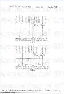 c) From position `b` fine tuning continues and reaches position `a` at which time D4 is set to 1, thus x = 1 and D5 is preset to count up from 0, thus, A = 0. The fine `DOWN` tuning is then repeated.
As in the case of `UP` fine control, the moment the DOWN control is released, the fine tuning stops, D3 stays at the value of x at that time, and D5 stays at the value of A at that time. These values of x and A are stored in the RAM 71 (FIG. 3).
Method of Frequency Tuning for even VHF Channels
In order to explain the method of frequency tuning for even VHF channels, let us take channel `6` as an example. The corresponding VCO frequency is 221.15MHz. The value of N can be calculated from equation 3 as follows: N = 221 - 1/2 = 110
tune Operation
When `TUNE` 68 (FIG. 3) is operated after setting `6` in the digital switch 69, (FIG. 3), the functions of the different stages of the system are as follows:
1. D2 divides by N = 110
2. d3 provides an additional count of 2. Thus x = 2.
3. (1) D5 is preset to down count from 15. (11) D4 is preset to down count from 8. (111) Total count of D4 and D5 i.e. A = 23.
Substituting the value of N, x and A in Equation 1, we obtain the value of fvco : fvco = 221.125MHz
This frequency is offset by 25KHz from the required frequency of 221.15MHz but is acceptable.
The operation of the `Fine UP` tuning and `Fine DOWN` tuning is similar to that described above for UHF and odd VHF channel selection except that in both cases counter D4 is set to count down from 8.
This results in a `Fine UP` frequency diagram as shown in FIG. 7 and a `Fine DOWN` frequency diagram as shown in FIG. 8.
It is especially envisaged that the digital synthesis frequency control system of FIG. 3 be implemented in integrated circuit form in which case it is envisaged that the following integrated circuit packages be used:
IC1 - A bipolar, 14 pin dual-in-line (DIL) package incorporating the ÷ 64 divider 52.
IC2 - A bipolar, 14 pin DIL package incorporating the - 15/16 divider 54, the phase/frequency comparator 59, part of the fixed divider 61 and the crystal oscillator 60.
IC3 - A MOS, 16 pin DIL package incorporating the programmable variable divider 57, the ROM 58 and fine tuning circuit 56, part of the fixed divider 61.
IC4 - A MNOS, 24 pin DIL package incorporating the RAM 71, the program address counter 73, the fine counter 72 and the channel counter/buffer 64.
IC5 (optional) incorporating the active filter 62, and band supply switching circuit for the tuner.
In the arrangement of FIG. 3, in order to facilitate programming of the ROM 58 and the RAM 71 with the minimum number of interconnecting lines, conventional multiplexing techniques may be used and additionally the RAM 71 may be arranged to operate in accordance with a read/erase/write cycle which is generated whenever a change in program number is detected or when the `TUNE` or FINE UP/DOWN controls are operated.
Conveniently also, it may be arranged that a `MUTE` output be generated which operates when a channel is changed to block the T.V. sound for a period say, of 200mS.
Although described as being applied to television receivers, the frequency synthesis tuning system described may have application in other forms of communications equipment such as radio receivers, radio transmitters, transmitter/receivers etc., and although `channel` tuning has been extensively considered, in other applications, simple frequency tuning may be used.
An electronically controllable tuning device includes a voltage controlled oscillator adapted to have an oscillation frequency controlled by a control voltage and simultaneously generate a fundamental wave of a predetermined frequency, a programmable frequency divider for dividing the fundamental wave frequency at a frequency division ratio corresponding to the control of a channel selection means and a phase locked loop adapted to compare the fundamental wave phase with the phase of the output of the programmable divider to generate a comparison output and feeding the comparison output back to the voltage controlled oscillator to control the output frequency of the voltage controlled oscillator. The tuning device further includes means for supplying as a local oscillation signal to an intermediate frequency generating mixer one of higher harmonic wave components of the fundamental wave.
 A digital phase control circuit which includes a controllable oscillator, a programmable divider coupled to the oscillator, a reference frequency source, a phase discriminator coupled to the outputs of the programmable divider and reference frequency source and means coupling the output of the phase discriminator to a control input of the oscillator. In addition to these components, an auxiliary circuit is provided which has its input coupled to the output of the phase discriminator and first and second outputs coupled to the reference frequency source and the programmable divider. The auxiliary circuit generates a first signal at the input of the reference frequency source when the phase difference between the signals at the outputs of the programmable divider and the reference frequency source is in one direction and a second signal at the second input of the programmable divider when the phase difference is in the opposite direction.
1. In a digital phase control circuit including a controllable oscillator having a control input; a programmable first divider having first and second inputs, said first input being coupled to the output of said oscillator; a reference frequency source comprising a second divider having an input; a phase discriminator having first and second inputs coupled to the outputs of said programmable first divider and said second divider respectively, said phase discriminator further having output means; and means coupling the output means of said phase discriminator to the control input of said controllable oscillator, the frequency of said oscillator being controlled in a direction determined by the direction of the phase deviation between the signals applied to the first and second inputs of said phase discriminator and compared therein; the improvement comprising:
an auxiliary circuit having input means coupled to the output means of said phase discriminator, a first output coupled to the input of said second divider comprising said reference frequency source and a second output coupled to the second input of said programmable first divider, said auxiliary circuit generating a first synchronizing signal at the input of said second divider when the phase difference between the signals at the ou
tputs of said programmable first divider and said second divider is in one direction and generating a second synchronizing signal at the second input of said programmable first divider when the phase difference between the signals at the outputs of said programmable first divider and said second divider is in the opposite direction thereby setting either said programmable first divider or said second divider, respectively, to a predetermined initial phase position, the divider set to said predetermined initial phase position being maintained in said position until the other divider reaches its predetermined initial phase position.
 2. The phase control circuit defined by claim 1 wherein said auxiliary circuit comprises a clock pulse generator for generating a signal at a predetermined interval after generation of a signal at the output of said phase discriminator, an auxiliary circuit output signal being generated at the input of said second divider or at the input of said programmable first divider only if the signal at the output of said phase discriminator is generated for an interval longer than said predetermined interval. 3. The phase control circuit defined by claim 2 wherein the output of said phase discriminator and the output of said auxiliary circuit each comprise a plurality of sequential pulses having a leading edge and a trailing edge, the leading edges of the pulses at the output of said auxiliary circuit occurring later than the leading edges of the corresponding pulses at the output of said phase discriminator, and the trailing edges of the corresponding pulses at both the output of the auxiliary circuit and the output of the phase discriminator coinciding. 4. The phase control circuit defined by claim 2 wherein said clock pulse generator receives counting pulses at a constant frequency, means are provided for releasing said clock pulse generator to count said counting pulses from its predetermined initial position when a signal is generated at the output of said phase discriminator and means are provided for coupling the signal at the output of said clock pulse generator to a disable input thereof to stop said counter. 5. A phase control circuit as defined by claim 4 wherein the output means of said phase discriminator comprises a first output at which pulses appear when the frequency of said oscillator is increasing and a second output at which pulses appear when the frequency of said oscillator is decreasing, and wherein said auxiliary circuit further includes a first gating circuit having first and second inputs coupled to the first and second outputs of said phase discriminator and an output coupled to a reset terminal of said clock pulse generator, second and third gating circuits for coupling the output of said clock pulse generator to the input of said second divider and to the second input of said programmable first divider, respectively, and fourth and fifth gating circuits coupling the first and second outputs of said
  phase discriminator to the inputs of said second and third gating circuits.
TELEFUNKEN PALCOLOR 8848J QUARTZ MEMORY CHASSIS 712A DPS2 TELEFUNKEN Superheterodyne receiver frequency tracking circuit:In a superheterodyne signal receiver including an input circuit arranged to be tuned to a frequency to be received and including a signal controllable variable reactance element presenting a reactance whose value is adjusted by a tuning signal and determines the frequency to which the input circuit is tuned, and a controllable local oscillator producing an alternating signal to be mixed with a received signal to produce an intermediate frequency received signal, a tracking circuit composed of: a first frequency control circuit including the local oscillator; a second frequency control circuit including a controllable sampling oscillator and a member connected to respond to the frequency of the output from the sampling oscillator to derive a signal related thereto and supplying that signal, as the tuning signal, to the controllable element; and a control signal generating unit generating first and second control signals and connected for supplying the first control signal to the first frequency control circuit for adjusting the frequency of the signal produced by the local oscillator, and for supplying the second control signal to the second frequency control circuit for adjusting the value of the tuning signal to tune the input circuit to a selected frequency, the generating unit maintaining a relationship between the first and second control signals such that the output frequency of the local oscillator is adjusted to the value corresponding to the received signal frequency to which the input circuit is tuned.
1. In a superheterodyne signal receiver including an input circuit arranged to be tuned to a frequency to be received and including a signal controllable variable reactance element presenting a reactance whose value is adjusted by a tuning signal and determines the frequency to which the input circuit is tuned, and a controllable local oscillator producing an alternating signal to be mixed with a received signal to produce an intermediate frequency received signal, a synchronizing circuit comprising: a first frequency control circuit including said local oscillator; a second frequency control circuit including a controllable sampling oscillator and means connected to respond to the frequency of the output from said sampling oscillator to derive a signal related thereto and supplying that signal, as the tuning signal, to said controllable element; and control signal generating means generating first and second control signals and connected for supplying said first control signal to said first frequency control circuit for adjusting the frequency of the signal produced by said local oscillator, and for supplying said second control signal to said second frequency control circuit for adjusting the value of said tuning signal to tune said input circuit to a selected frequency, said generating means maintaining a relationship between said first and second control signals such that the output frequency of said local oscillator is adjusted to the value corresponding to the received signal frequency to which said input circuit is tuned, wherein each said frequency control circuit includes converter means connected to provide an output signal representative of the frequency of the signal produced by its associated oscillator, and oscillator control means having a first input connected to receive the output signal provided by its associated converter means, a second input connected to receive its respective control signal and an output connected to supply its associated oscillator with a setting signal which is dependent on a relation between the signals at its first and second inputs for establishing a linear relationship between its respective control signal and the frequency produced by its respective oscillator, said synchronizing circuit further comprises a source of an addition a.c. signal, and said converter means of at least one said circuit has at least two inputs one of which is connected to receive a signal derived from the signal at the output of its associated oscillator and the other of which is connected to receive the additional a.c. signal and acts to cause its output signal to be dependent on a relationship between the frequencies of the signals applied to its two inputs.
2. In a superheterodyne signal receiver input section including: an input circuit, arranged to be tuned to the frequency of a signal to be received and containing a controllable reactance the value of which is adjusted by a tuning signal and determines the frequency to which the input circuit is tuned; a controllable local oscillator producing an alternating signal to be mixed with a received signal supplied by the input circuit to produce an intermediate frequency received signal; a first frequency control loop composed of the local oscillator, a first converter connected to provide an output signal representative of the frequency of the signal produced by the local oscillator, and first oscillator control means having a first input connected to receive the output signal provided by the first converter, a second input connected to receive a first control signal and an output connected to supply the local oscillator with a setting signal to adjust the frequency of the signal produced by the local oscillator as a function of a relation between the first control signal and the output signal provided by the first converter, with the local oscillator, first converter and first oscillator control means being connected together in a loop; a second frequency control loop including a controllable sampling oscillator containing a controllable reactance the value of which determines the frequency of the signal produced by the sampling oscillator, a second converter connected to provide an output signal representative of the frequency of the signal produced by the sampling oscillator control means having a first input connected to receive the output signal provided by the second converter, a second input connected to receive a second control signal and an output connected to supply the sampling oscillator with a setting signal to adjust the frequency of the signal produced by the sampling oscillator as a function of a relation between the second control signal and the output signal provided by the second converter, and means connected to supply the tuning signal to the input circuit, the value of which tuning signal is a function of the frequency of the signal being produced by the sampling oscillator, with the sampling oscillator, second converter and second oscillator control means being connected together in a loop; and control signal generating means including a source of a reference signal and means for causing the first and second control signals to be functions of the reference signal and to be so related to one another that the input circuit is tuned to a received signal frequency corresponding to the output frequency of the local oscillator, the improvement wherein said reference signal source comprises a source of an a.c. reference frequency signal, and a third converter connected to receive the reference frequency signal and to provide said reference signal at its output for compensating undesirable changes in the output signals produced by said first and second converters as a result of external adverse influences.
3. Circuit arrangement as defined in claim 2 wherein said control signal generating means comprise a common control element constituting the source of both said first and second control signals.
4. Circuit arrangement as defined in claim 3 wherein said control signal generating means further comprise signal modifying means connected to subject the output of said common control element to arithmetic operations for giving said first control signal a value which causes the output frequency of said local oscillator to be offset from the corresponding received signal frequency by a constant amount corresponding to the intermediate frequency value and for giving said second control signal a value which causes said tuning signal to tune said input circuit to a frequency corresponding to the frequency of the output of said local oscillator and differing from said local oscillator frequency by the intermediate frequency.
5. Circuit arrangement as defined in claim 4 wherein each of said first and second converters includes means establishing a linear relationship between its respective control signal and the frequency produced by its respective oscillator.
6. Circuit arrangement as defined in claim 5 wherein at least one of said control signals is an analog signal.
7. Circuit arrangement as defined in claim 6 wherein at least one said oscillator control means comprises a comparator.
8. Circuit arrangement as defined in claim 7 wherein, in said at least one loop, said comparator has two inputs, one of which is connected to the output of said converter in the same loop, said comparator having an output connected to control the frequency of said oscillator associated with the same loop, and said control signal for said loop is supplied to the second input of said comparator.
9. Circuit arrangement as defined in claim 5 wherein said converter of at least one said loop has at least two inputs for receiving a signal from the oscillator associated with said loop and the a.c. reference frequency signal signals and acts to produce an output signal having a d.c. component which varies in dependence on a relationship between the frequencies of the two input signals.
10. Circuit arrangement as defined in claim 9 wherein said third converter is connected to said reference frequency source for producing an output signal having a d.c. component proportional to the reference frequency and constituting said reference signal.
11. Circuit arrangement as defined in claim 9 wherein said converter of said at least one loop produces an output signal which changes only when there is a change in the frequency relationship of the two a.c. input signals and in proportion to this relationship.
12. Circuit arrangement as defined in claim 11 wherein said converter of said at least one loop operates to reverse the frequency relationship to which the change in the direct component of the output signal is proportional when the connections of the input signals to the two inputs of said converter are interchanged.
13. Circuit arrangement as defined in claim 9 wherein said converter of said at least one loop has a further input connected to receive a further a.c. input signal for further controlling the d.c. component of the output signal of said converter as a function of the frequency of the further input signal.
14. Circuit arrangement as defined in claim 9 wherein variation in the d.c. component of the output signal of said converter of said at least one loop is proportional to changes in the duty ratio of at least one of its input signals.
15. Circuit arrangement as defined in claim 9 wherein the d.c. component of the output of said converter of said at least one loop varies according to the relationship V=K1 +K2.f1 /f2, where V is the value of the d.c. component, K1 and K2 are constants, f1 is the frequency of the output of its respective oscillator and f2 is the frequency of the output of said reference frequency source.
16. Circuit arrangement as defined in claim 2 wherein all of said converters are structurally and functionally identical.
17. Circuit arrangement as defined in claim 2 or 16 wherein said controllable reactances of said input circuit and said sampling oscillator are constituted such that the values of said reactances vary in a constant ratio to one another in response to changes in the value of said second control signal.
18. Circuit arrangement as defined in claim 17 wherein said controllable reactances of said input circuit and said sampling oscillator are identical in their design and response characteristics.
19. Circuit arrangement as defined in claim 18 further comprising a single semiconductor chip presenting two identically constructed semiconductor varactor diodes, and wherein each said diode constitutes a respective one of said controllable reactances.
20. Circuit arrangement as defined in claim 19 wherein the capacitances of said two diodes bear a constant ratio to one another and further comprising two capacitors each connected in parallel with a respective diode, the values of the capacitances of said capacitors being in said constant ratio to one another.
21. Circuit arrangement as defined in claim 18 wherein said controllable reactances present controllable capacitances having capacitance values which bear a constant ratio to one another and further comprising two capacitors each connected in parallel with a respective controllable capacitance, the values of the capacitances of said capacitors being in said constant ratio to one another.
22. Circuit arrangement as defined in claim 17 wherein said controllable reactances present controllable capacitances having capacitance values which bear a constant ratio to one another and further comprising two capacitors each connected in parallel with a respective controllable capacitance, the values of the capacitances of said capacitors being in said constant ratio to one another.
23. Circuit arrangement as defined in claim 17 further comprising a single semiconductor chip presenting two identically constructed semiconductor varactor diodes, and wherein each said diode constitutes a respective one of said controllable reactances.
24. Circuit arrangement as defined in claim 2 or 16 wherein said controllable reactances of said input circuit and said sampling oscillator are identical in their design and response characteristics.
25. Circuit arrangement as defined in claim 2 or 16 further comprising a single semiconductor chip presenting two identically constructed semiconductor varactor diodes, and wherein each said diode constitutes a respective one of said controllable reactances.
26. Circuit arrangement as defined in claim 2 or 16 wherein said controllable reactances present controllable reactances present controllable capacitances having capacitance values which bear a constant ratio to one another and further comprising two capacitors each connected in parallel with a respective controllable capacitance, the values of the capacitances of said capacitors being in said constant ratio to one another.
It is known that frequency synchronism must exist between the oscillator and the input circuit of a superheterodyne receiver.
In order to attain the required synchronism between oscillator and input circuit, various techniques are employed. For example, it can be attempted to achieve the desired synchronism by specially cutting the discs of the rotary tuning capacitor. However, for electronic tuning systems varactor diodes which have specially adapted capacitance/voltage characteristics are not available. For this reason, tuning systems with varactor diodes employ the known threepoint tracking which, however, permits optimum tracking, or synchronization only at three points of the frequency range. Even with precisely identical characteristics of the tuning elements or diodes, there occur synchronization deviations which result in sensitivity breaks within the tuning range. Moreover, inequality of the characteristics and deviations in the capacitance value of the padding capacitor produce additional deviations and thus increase the problem.
SUMMARY OF THE INVENTION
Objects of the present invention are to provide improved synchronization compared to the known tracking circuits and to eliminate the deviations which, when three-point synchronization is employed, inherently occur in such known circuits across the tuning frequency band.
This and other objects are achieved, according to the present invention, by the provision, in or for a superheterodyne signal receiver including an input circuit arranged to be tuned to a frequency to be received and including a signal controllable variable reactance element presenting a reactance whose value is adjusted by a tuning signal and determines the frequency to which the input circuit is tuned, and a controllable local oscillator producing an alternating signal to be mixed with a received signal to produce an intermediate frequency received signal, of a tracking circuit composed of: a first frequency control circuit including the local oscillator; a second frequency control circuit including a controllable sampling oscillator and means connected to respond to the frequency of the output from the sampling oscillator to derive a signal related thereto and supplying that signal, as the tuning signal, to the controllable element; and control signal generating means generating first and second control signals and connected for supplying the first control signal to the first frequency control circuit for adjusting the frequency of the signal produced by the local oscillator, and for supplying the second control signal to the second frequency control circuit for adjusting the value of the tuning signal to tune the input circuit to a selected frequency, the control signal generating means maintaining a relationship between the first and second control signals such that the output frequency of the local oscillator is adjusted to the value corresponding to the received signal frequency to which the input circuit is tuned.
As is known, tuning circuits have the object of tuning the resonant circuits of selective amplifiers and/or oscillators to a given resonant frequency. In a known tuning circuit, the adjustment to synchronous operation in each circuit takes place via a tuning coil and a particular trimmer capacitor. In the known tuning circuit arrangement a multiply repeated adjustment of the inductance and the capacitance is required for adjustment to synchronous operation, because the setting of the trimmer capacitors again changes the resonant frequency of the frequency previously set inductively.
SUMMARY OF THE INVENTION
It
is an object of the invention to provide a tuning circuit arrangement with simplified adjustment.According to a first aspect of the invention, there is provided a tuning circuit arrangement comprising one or more tuned circuits, tuning diodes in said tuned circuits for tuning the frequency range of said tuned circuits and means for varying the tuning voltage of said tuning diodes for providing exclusive variation of the tuned circuit capacitance of said tuned circuit.
According to a second aspect of the invention, there is provided a tuning circuit arrangement comprising one or more tuning circuits, in which tuning diodes are provided for the purpose of tuning the frequency range and in which the tuned circuit adjustment takes place by changing the tuned circuit inductance and the tuned circuit capacitance, characterized in that the adjustment in capacitance takes place exclusively by varying the tuning voltage for the tuning diode(s).
BRIEF DESCRIPTION OF THE DRAWINGS
The invention will now be described in greater detail, by way of example, with reference to the drawings in which:
FIG. 1 is a circuit diagram showing a first form of circuit arrangement in accordance with the invention as applied to two resonant circuits;
FIG. 2 is a circuit diagram similar to FIG. 1 but showing the arrangement applied to n resonant circuits;
FIG. 3 is a circuit diagram similar to FIG. 1 but showing the arrangement with a different form of adjustment;
FIG. 4 is a circuit diagram similar to FIG. 2 in which the arrangement of FIG. 3 is applied to n resonant circuits;
FIG. 5 is a circuit diagram showing a part of the arrangement showing a different form of adjusting circuitry;
FIG. 6 is a circuit diagram similar to FIG. 5 but showing a still further form of adjusting circuitry;
FIG. 7 is a block diagram of part of the arrangement provided with temperature compensation and,
FIG. 8 is a block diagram similar to FIG. 7 but including a decoupling circuit.
DESCRIPTION OF THE PREFERRED EMBODIMENTS
In a tuning circuit arrangement of the type mentioned at the beginning it is proposed in accord
 ance with the invention and in order to solve the object that the adjustment in capacitance should take place exclusively by variation of the tuning voltage for the tuning diode(s).
The essence of the invention on the one hand consists in that special trimmer capacitors for achieving an adjustment in capacitance are omitted and that the adjustment in capacitance takes place exclusively by variations of the tuning voltage for the tuning diode(s) which is in contrast to the known method, and does not take place by means of trimmer capacitors. On the other hand, the invention does not require any repetitive adjustment of the tuned circuits of the tuning circuits.
The tuning circuit arrangement in accordance with the invention makes it possible to reduce considerably the required maximum tuning voltage. With the tuning circuit arrangement in accordance with the invention it is possible to operate with small tuning voltages even when using tuning diodes having abrupt pn junction. The sought after simplification of the adjustment can be achieved by means of the fact that the capacitative adjustment does not influence the previously operated adjustment in inductance.
In the tuning circuit arrangement according to the invention potentiometers, for example, are provided in order to adjust the capacitance. There is the possibility of using the same adjusting means for adjusting the capacitance of two or more tuned circuits. Similarly, the same adjustment means may serve to adjust the capacitance of several tuned circuits having varying relative frequency variation.
In accordance with a further refinement of the invention a circuit arrangement for producing minimum and maximum tuning potentials is provided which is constructed so that the potentials produced by it have such a temperature dependence that the effect of temperature on the tuning circuit is compensated.
It is advisable to connect a decoupling circuit between the means for adjusting capacitance and the 6 tuning potentiometers, the decoupling circuit reducing the electrical load on the tuning potentiometer through the adjustment means. In accordance with an embodiment of the invention, precautions are taken to ensure that one of the two potentials applied to an adjustment potentiometer, does not change during adjustment.
The adjustment potentiometer or potentiometers are connected for example between a point in the circuit at which the variable tuning potential is available and a point in the circuit at which the minimum tuning potential is available. There is also the possibility of connecting the adjustment potentiometer or potentiometers between a point in the circuit at which the variable tuning potential is available and a point in the circuit at which the maximum tuning potential is available.
Referring now to the drawings, FIG. 1 shows an electronic tuning circuit in accordance with the inv
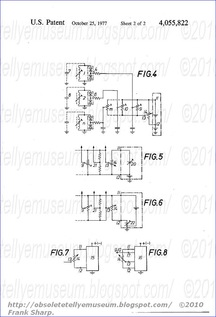 ention which operates with tuning diodes. The tuning circuit of FIG. 1, which is for example a component of a VHF tuner, consists of two variable-frequency resonant circuits and in fact an oscillator circuit 1 and a resonant circuit 2 for selecting the input signal. The oscillator circuit comprises an inductance 3 and a tuning diode 4, which is a double diode in this embodiment. The resonant circuit 2 comprises an inductance 5 and a tuning diode 6, which in this embodiment is also a double diode. As may be seen from FIG. 1, neither of the two resonant circuits 1 and 2 has a trimmer capacitor. Of course, parallel to the resonant circuits there are unavoidable circuit capacitances 7 and 8 which are shown in broken lines.
The two resonant circuits 1 and 2 must be adjusted to achieve synchronous operation. In accordance with the invention the adjustment potentiometers 9 and 10 are provided for this purpose. The adjustment potentiometers 9 and 10 are connected in parallel with one another in the embodiment of FIG. 1. Two limiting potentials are required for the tuning circuit; in fact the largest potential U max at point 11 and the smallest potential U min at point 12. In the embodiment of FIG. 1 the two adjustment potentiometers 9 and 10 lie between the wiper contact 13 of the tuning potentiometer 14 and the point 12 having the potential U min . The tuning potentiometer 14 lies between the points 11 and 12, i.e. between the maximum potential U max and the minimum potential U min . The maximum tuning potential U max and the minimum tuning potential U min are in fact linked together, yet they are produced in a separate circuit arrangement. This is indicated symbolically in FIG. 1 by means of the two voltage sources 23 and 24. The minimum tuning potential U min is therefore not derived via a purely ohmic voltage divider from the maximum tuning potential U max .
In the tuning circuit of FIG. 1, in the case where the tuning potentiometer 14 is set to the minimum tuning voltage, the voltages taken from the adjustment potentiometers 9 and 10 are not influenced by the settings of the adjustment potentiometer. Therefore, if the wiper contact 13 of the tuning potentiometer 14 is located at the lowest position then no matter how the adjustment potentiometers 9 and 10 are rotated the adjustment voltages for the tuning diodes will not be influenced by this. This has the consequence that setting in the upper frequency range has no influence on the previously set lower frequency. The adjustment of the lower frequency is only dependent on the inductance adjustment of the inductances 3 and 5.
The tuning circuit of FIG. 2 is distinguished from the tuning circuit of FIG. 1 by the fact that instead of only two resonant circuits n resonant circuits are provided and, instead of only two adjustment potentiometers, m adjustment potentiometers are provided. m may be smaller than n if not merely one resonant circuit but more than one resonant circuit is adjusted by means of a single adjustment potentiometer.FIG. 3 shows an embodiment of the invention in which in contrast to FIGS. 1 and 2 the adjustment potentiometers 9 and 10 lie between the wiper contact 13 of the tuning potentiometer 14 and point 11 having the potential U max . In this case, the adjustment in inductance takes place in the upper frequency and the adjustment in capacitance takes place in the lower frequency by means of the adjustment potentiometers 9 and 10.
The tuning circuit of FIG. 4 is distinguished from the tuning circuit of FIG. 3 by the fact that, instead of only two resonant circuits, again n resonant circuits are provided and instead of only two adjustment potentiometers m adjustment potentiometers are provided.
According to FIG. 5 the adjustment in capacitance is undertaken for the upper frequency by setting the maximum tuning potential. While in the tuning circuits of FIGS. 1 to 4 the adjustment of the individual tuned circuits is independent, in the arrangement of FIG. 5 the setting of the maximum tuning potential effects all tuned circuits. The setting of the maximum tuning potential takes place in the arrangement of FIG. 5 by means of the voltage source 20. The voltage supplying the tuning diodes may for example be taken from the wiper contact 13 of the tuning potentiometer 14, from a fixed voltage divider 21 or from the wiper contact of the adjustment potentiometer 9. Several adjustment potentiometers may be provided instead of only one adjustment potentiometer.
The arrangement of FIG. 6 is distinguished from the arrangement of FIG. 5 by the fact that the minimum tuning potential is made settable instead of the maximum tuning potential for the purpose of adjustment. Moreover, in the arrangement of FIG. 6, the network which comprises the voltage divider 21 and the adjustment potentiometer 9, is connected between the wiper contact 13 of the adjustment potentiometer 14 and the maximum tuning potential 11.
According to FIG. 7, the maximum and minimum tuning potential is produced by means of a circuit arrangement 15 which has the object of supplying such a temperature effect of the potential that the temperature effect of the tuning circuit is compensated by an appropriate temperature effect of the potentials.
The arrangement 16 of FIG. 8 also produces the minimum and maximum tuning potentials at the points 11 and 12 as well as the effective temperature on these potentials which is required for temperature compensation of the tuning circuit. In addition, the arrangement 16 contains a decoupling circuit which lies between the wiper contact 13 of the tuning potentiometer 14 and the adjustment potentiometers 9 and 10.
The tuning circuit dealt with in the embodiments is developed for positive tuning potentials. In a similar manner, the tuning circuits of the invention may also be designed for negative tuning potentials.
It will be understood that the above description of the present invention is susceptible to various modification changes and adaptations.
TELEFUNKEN PALCOLOR 8848J QUARTZ MEMORY CHASSIS 712A DPS2 TELEFUNKEN PLL SYNTHESIZER PLESSEY CHIPSET CT1112 CT1111 Digital phase control circuit including an auxiliary circuit:

This application describes a receiver in which channel selection is controlled by a frequency synthesizer a sweep of available channels is made by a channel selecting arrangement and this sweep is arranged to be stopped when a signal is received. When the sweeping is stopped a fine tuning arrangement takes control to respond to the frequency of the received signal and to compensate for any drift of that signal. A tuning circuit for a high frequency receiver in which the received frequency is determined by a voltage-controlled oscillator, the present tuning frequency is indicated by a counter connected to the oscillator and producing a representation of each digit of the decimal number identifying the current received frequency, representations of the digits of the number identifying the desired received frequency are fed in via a rotary switch , and the decimal number representations are compared in a comparator to produce a control voltage that brings the oscillator frequency to the desired value, and in which the comparator is capable of comparing only one digit of the number representations at a time and receives the digits of corresponding significance in sequence, starting with the most significant digit, and the rate at which the control voltage is varied is made inversely proportional to the number of changes in the direction of the inequality of the digits of one of the number representations being compared relative to the corresponding digits of the other number representation being compared.
1. In a tuning circuit for a high frequency receiver, which circuit includes a voltage controllable superheterodyne oscillator arranged to receive a control voltage and to produce an oscillation whose frequency is determined by the value of the control voltage and determines the broadcast frequency to which the receiver is tuned, a counter connected to sense the frequency of the oscillations being generated by the oscillator and to produce therefrom a count state in the form of representations of the digits of a first decimal number identifying the broadcast frequency to which the receiver is currently tuned, input means for generating representations of the digits of a second decimal number identifying the broadcast frequency to which it is desired to tune the receiver, and a comparison circuit for comparing the decimal number representations being produced by the counter and the input means in order to vary the control voltage in a direction to cau

2. An arrangement as defined in claim 1 wherein said adjustment means comprises a sequence counter connected for counting the number of such sequences and having its count state set to zero at the beginning of each tuning operation.
3. An arrangement as defined in claim 2 wherein said adjustment means further comprises a logic gate connected to the output of said sequence counter and having a number of outputs equal to a selected number of desired control voltage variation rates, said gate being arranged to provide a certain logic potential at one of its outputs in dependence on the count state of said sequence counter.
4. An arrangement as defined in claim 3 wherein said comparison circuit includes an amplifier arranged to provide an output signal which effects variation of the control voltage, and said adjustment means further comprise a plurality of resistors having respectively different resistance values and each connected between a respective output of said gate and said amplifier for causing the control voltage variation rate to have a value determined by the resistance value of that resistor whose associated gate output is providing the certain logic potential.
 5. An arrangement as defined in claim 4 wherein the comparison circuit further includes a capacitor connected to receive the output signal from said amplifier so that the voltage thereacross constitutes the control voltage, said amplifier being arranged for supplying said capacitor with a charging or discharging current proportional to the current flowing through that one of said resistors whose associated gate output is providing the certain logic potential.
 6. An arrangement as defined in claim 4 wherein said amplifier is connected to said second and third comparator outputs for causing the direction of variation of the control voltage to be determined on the basis of which one of said second and third comparator outputs is providing a signal.
7. An arrangement as defined in claim 4 wherein said gate is arranged to cause its outputs to be blocked at a selected maximum count state of said sequence counter for preventing current flow through any of said resistors.
8. An arrangement as defined in claim 4 wherein said logic gate is arranged to have its outputs blocked when there is coincidence between all digits of the two numbers.
9. An arrangement as defined in claim 2 wherein said adjustment means comprises a programmable frequency divider connected to have its dividing ratio determined by the counter state of said sequence counter in a manner such that the dividing ratio increases with increasing counter state.
10. An arrangement as defined in claim 9 wherein said adjustment means further comprises means for producing square wave oscillations of a constant frequency connected to feed such oscillations to said divider.
11. An arrangement as defined in claim 10 wherein said adjustment means comprises a digital-analog converter connected to the output of said divider and providing an output voltage whose value determines the magnitude of the rate of variation of the control voltage.
Description:
BACKGROUND OF THE INVENTIONThe present invention relates to a tuning circuit for a high frequency receiver having a superheterodyne oscillator whose frequency can be varied by means of a tuning voltage in order to tune the receiver to a desired station.
In such circuits, the tuning voltage, which is a direct voltage, is generated by a comparison circuit which effects a comparison between two numbers. The first number identifies the counter state of a counting device which periodically counts the oscillations of the superheterodyne oscillator on the basis of the intermediate frequency. This number thus constitutes the received frequency, or possibly the received channel or station. The second number is fed to the comparison circuit via an input keyboard provided with a series-connected coder and identifies the desired channel or station to which the receiver is to be tuned. The comparison circuit has three outputs, one output for the c
omparison result "equality" and one each for the two non-equality results "greater" and "less". In the circuit disclosed in U.S. application Ser. No. 708,754, filed by the present applicant and Dieter Rottmann and Stephan Wuttke on July 26, 1976, the comparison is effected by a multiplex operation and the comparison circuit is composed of only a single comparator which can effect a comparison with respect to only one digit, or level of significance, of the numbers at a time. This comparator receives, in succession, the representations of the digits of the two numbers to be compared, beginning with the most significant digit.
If in the described tuning circuit the two numbers are unequal, the tuning circuit, and thus the frequency of the superheterodyne oscillator, is changed until the frequency identified by the number fed in has been attained. The rate at which the tuning voltage changes is relatively great if the two numbers to be compared differ from one another in all digit positions. The rate of change becomes less as more digits of the two numbers, beginning with the most significant digit, become equal. When all digits are equal, the frequency will no longer be changed. The tuning rate thus decreases as more digits become identical, this result being a function of the evaluation circuit provided in the above-cited application. The successive rates there are proportional to 1/2 . . . 1/n, where n = number of digit positions, e.g. 5. It has been found that this tuning process takes a relatively long time, which many operators consider to be a drawback.
SUMMARY OF THE INVENTION
It is therefore an object of the present invention to shorten the time required for the tuning process.
These and other objects are achieved, in a tuning circuit for a high frequency receiver, which circuit includes a voltage controllable superheterodyne oscillator arranged to receive a control voltage and to produce an oscillation whose frequency is determined by the value of the control voltage and determines the broadcast frequency to w
hich the receiver is tuned, a counter connected to sense the frequency of the oscillations being generated by the oscillator and to produce therefrom a count state in the form of representations of the digits of a first decimal number identifying the broadcast frequency to which the receiver is currently tuned, input means for generating representations of the digits of a second decimal number identifying the broadcast frequency to which it is desired to tune the receiver, and a comparison circuit for comparing the decimal number representations being produced by the counter and the input means in order to vary the control voltage in a direction to cause those two number representations to coincide, the comparison circuit including a comparator capable of comparing the representations of one digit of each of two numbers and having two inputs connected, respectively, to the counter and to the input means, the comparator being arranged to receive, at one of its inputs, each digit representation produced by the counter, starting with the most significant digit, and, at the other of its inputs, simultaneously therewith each digit representation of corresponding significance generated by the input means, the comparator including a first output providing a signal when the digit representations at its inputs are identical, a second output providing a signal when the digit representation at its one input represents a value larger than that of the digit representation at its other input, and a third output providing a signal when the digit representation at its one input represents a value smaller than that of the digit representation at its other input, by the provision of tuning voltage adjustment means connected to the comparator outputs and responsive to the number of sequences of termination of a signal at one of the second and third outputs and subsequent initiation of a signal at the other of the second and third outputs for varying the control voltage at a rate inversely proportional to such number of sequences. Thus, in the present invention, the number of reversals of the inequality results determines the respective level of the rate of change of the tuning voltage. The greater the number of changes in inequality results, i.e. the smaller the difference between the two numbers, the lower will be the tuning rate.
In the tuning circuit described in the above-cited earlier U.S. application, there is also a reduction in the tuning rate as a result of different stages of the rate of change, but the differences between the various stages are only slight. The reason for this is that the tuning voltage which effects a change in frequency is generated by means of an integrating member, or low-pass filter, from pulses which vary in repetition rate by a maximum of, for example, 1:5 per unit time, corresponding to the number of digit positions. The direct voltage at the output of the integrating member can therefore only take on values which correspond to a linear graduation 0, 1, 2, . . . n.
In the present invention, however, it is possible to provide practically any difference between the stages, or graduated variations, in the rate of change so that the tuning process can be optimized.
The periodical "Funkschau" 1974, Issue No. 3, at page 93, discloses a circuit which assigns different significances to individual decades during the comparison of two numbers associated with generation of the tuning voltage. However, this comparison of the two numbers is not performed in a multiplex operation but in a parallel operation. Therefore each decade must have its own comparator, causing the known tuning circuit to be very expensive.

1. A receiver comprising a frequency synthesizer controlled channel selection means which includes a controllable oscillator having a frequency and providing an output signal, dividing means including a
 n adjustable divider for dividing the output signal to obtain a divided output signal, a reference signal source for providing a reference signal, a comparator for comparing the reference signal with the divided output signal and for providing a control signal to control the controllable oscillator, fine tuning means for fine tuning the frequency of the controllable oscillator, means for initiating a sweep of available channels by the channel selection means, means for stopping the sweep on reception of a signal by said receiver on one of the available channels, and control means operable on cessation of sweeping and responsive to the frequency of the signal for controlling the fine tuning means to compensate for frequency drift of the signal. 2. A receiver as claimed in claim 1 wherein the receiver is a television receiver. 3. A receiver as claimed in any one of claims 1 or 2 wherein the control means comprises level detector means for receiving a frequency representative signal having a level which is representative of the frequency of the received signal so as to monitor frequency drift of said received signal, and for providing an output signal when a predetermined frequency drift is detected. 4. A receiver as claimed in claim 3 wherein two level comparators are provided, each of said two level comparators receiving the frequency representative signal and a respective reference level and providing an output representative of an upward and downward frequency drift, respectively, exceeding predetermined limits. 5. A receiver as claimed in claim 4 wherein the frequency representative signal is provided by automatic frequency control (A.F.C.) means for automatically controlling the frequency of the received signal. 6. A receiver as claimed in claim 5 wherein the automatic frequency control means comprises an A.F.C. discriminator. 7. A receiver as claimed in claim 3 wherein the frequency representative signal is provided by automatic frequency control (A.F.C.) means for automatically controlling the frequency of the received signal. 8. A receiver as claimed in claim 3 wherein the control means controls the fine tuning means via a signal path which includes blocking means for blocking said signal path until said signal is received. 9. A receiver as claimed in claim 3 wherein said channel selection means has a control input, and the means for initiating the sweep comprises an operator control coupled to the control input of the channel selection means, and the means for stopping the sweep is operative to isolate the operator control from the control input of the channel selection means. 10. A receiver as claimed in claim 3 wherein the means for stopping the sweep includes detecting means for detecting the reception of said signal. 11. A receiver as claimed in claim 10 wherein the detecting means comprises a synch comparator operative to compare video signals with line flyback signals and to provide an output signal having a level indicative of the reception of said signal. 12. A receiver as claimed in claim 1 wherein the control means controls the fine tuning means via a signal path which includes blocking means for blocking said signal path until said signal is received. 13. A receiver as claimed in claim 12 wherein the blocking means comprises gate means connected to said signal path and receiving, as a second input, a reception signal indicative of the reception of said signal. 14. A receiver as claimed in claim 1 wherein said channel selection means has a control input, and the means for initiating the sweep comprises an operator control coupled to the control input of the channel selection means, and the means for stopping the sweep is operative to isolate the operator control from the control input of the channel selector means. 15. A receiver as claimed in claim 14 wherein the operator control is coupled to the channel selection means via gating means operative for opening on operation of the operator control. 16. A receiver as claimed in claim 15 wherein the means for stopping the sweep is arranged to provide a blocking signal operative to block the gating means on receipt of said signal. 17. A receiver as claimed in claim 1 wherein the means for stopping the sweep includes detecting means for detecting the reception of said signal. 18. A receiver as claimed in any one of claims 2 or 17 wherein the detecting means comprises a synch comparator operative to compare video signals with line flyback signals and to provide an output signal having a level indicative of the reception of said signal.
Description:
This invention relates to a receiver arrangement incorporating frequency synthesizer controlled channel selection. The invention is particularly although not exclusively applicable to a television receiver. The term channel is used herein in a general sense to refer to an available reception frequency.
In our co-pending G.B. patent application No. 32419/16 corresponding to U.S. Pat. No. 4,123,724 of Das et al, issued on Oct. 31, 1978, there is described a frequency synthesizer control arrangement suitable for use in a television receiver for effecting frequency control of its local oscillator for the purpose of channel selection.
In that application two methods of channel selection have been described. The first method is to select the channel number in a digital switch and then to enter the channel numbers by pressing the TUNE control.
The second method is to effect a sweep through the whole range of channel numbers until a required number is reached. In both methods fine tuning is effected by operation of the provided fine tune controls.
In the channel sweep tuning method disclosed, a user has to keep the tuning control operated until the required channel is reached at which point the control must be immediately released. This can be a disadvantage if the user is not familiar with the channel numbers of his area, he must watch the T.V. screen and release the control at the moment a picture appears.
This invention seeks to provide a receiver arrangement employing frequency synthesizer controlled channel selection in which the above mentioned disadvantage is mitigated.
According to this invention there is provided a receiver comprising frequency synthesizer controlled channel selection means which includes a fine tuning arrangement; means for initiating a sweep of available channels by the channel selection means; means for stopping the sweep on reception of a signal and means, operable on cessation of sweeping and responsive to the frequency of the signal, and arranged to control the fine tuning arrangement to compensate for frequency drift of the signal.
The receiver may be in the form of a television receiver.
The means operable a cessation of sweeping may comprise level detector means arranged to receive a signal whose level is representative of the frequency of the received signal and to provide an output signal when a predetermined frequency drift is detected.
In a preferred form two level comparators are provided each arranged to receive the frequency representative signal and a respective reference level and to provide an output respectively representative of an upward and downward frequency drift exceeding predetermined limits.
The signal whose level is representative of the frequency of the received signal may be provided by automatic frequency control (A.F.C.) means conveniently in the form of an A.F.C. discriminator.
The means operable or cessation of sweeping may be arranged to control the fine tuning arrangement via a signal path which includes means for blocking said signal path until the said signal is received.
The means for blocking may be in the form of gate means connected to the said signal path and arranged to receive a second input a signal indicative of the receipt of the said signal.
The means for initiating a sweep may comprise an operator control coupled to control input means of the channel selection means, and the means for stopping sweeping is operative to isolate the operator control from the said control input means.
The operator may be coupled to the channel selection means via gating means operative to open an operation of the operator control and the means for stopping sweeping may provide a signal operative to block the gating means or receipt of the said signal.
The means for stopping sweeping may include means for detecting the reception of the said signal which in a preferred form of television receiver comprises a sync comparator operative to compare video signals with line flyback signals and to provide an output signal whose level is indicitive of the reception of the said signal.
The invention will now be further described with reference to the accompanying single FIGURE drawing which shows schematically a television receiver in accordance with the invention.
Referring to the drawings there is shown a television receiver which has a local oscillator and other standard television components such as i.f. amplifier and sound and vision detection and reproduction circuits, all shown within rectangular box referenced 1. A frequency synthesizer unit 2 controls the frequency of the local oscillator in order to provide channel selection.
The frequency synthesizer unit 2 has a fine tuning arrangement and may conveniently be as described in our co-pending application No. 32419/76 corresponding to U.S. Pat. No. 4,123,724 of Das et al, issued on Oct. 31, 1978,.
The frequency synthesizer unit 2 is capable of effecting a sweep of available channels and has three inputs which correspond to inputs to the synthesizer described in the co-pending application. A first input 3 is a channel sweep/fine tuning input and when an appropriate signal level is applied to this input the frequency synthesizing unit 2 is caused to sweep through available reception channels. In the absence of a suitable signal level to the input 3 the frequency synthesizer unit 2 is only operative in the fine tune mode in a manner to be described.
The second and third inputs 4 and 5 are respectively up and down control inputs. The up and down control inputs 4 and 5 perform a dual function of indicating to the frequency synthesizer unit 2 during channel sweeping the direction in which sweeping is to be effective and also act as fine tuning signal inputs when the synthesizer is operating in the fine tuning mode.
To initiate sweeping two operator controls are provided in the form of push button switches 6 and 7 the switch 6 being a sweep up switch while the switch 7 is a sweep down switch. The switches 6 and 7 are operative to connect potentials applied at terminals 8 and 9 respectively to the SET input of flip-flops 10 and 11 respectively. The terminal 8 connected via the switch 6 to the SET input of the flip-flop 10 is also connected via the switch to the RESET input of the flip-flop 11 whilst the terminal 9 is similarily connected to the RESET input of the flip-flop 10 so that whenever one of the two flip-flops is SET the other is automatically RESET. Typically potentials of 5 volts are applied to the terminals 8 and 9.
The flip-flops 10 and 11 have Q outputs respectively connected to one input of NOR gates 12 and 13 which have outputs connected via one position of respective two position auto/manual switches 14 and 15 the wipers of which are connected to respective inputs of an OR gate 16 whose output is connected to the channel sweep/fine tuning input 3 of the frequency synthesizer unit 2. The wiper of the switch 14 is also connected to one input of an OR gate 17 whose output is connected to the input 4 of the synthesizer unit 2 whilst the wiper of the switch 15 is connected to one input of an OR gate 18 whose output is connected to the input 5 of the synthesizer unit 2.
In the second position of each switch 14 and 15 the potentials applied to the terminals 8 and 9 are applied to the gate 16 and to the gates 17 and 18 respectively. The terminals 8 and 9 are also connected via respective switches 6 and 7 to respective inputs of an OR gate 19 whose output is operative to trigger a monostable multivibrator 20 the output of which is connected to one input of an AND gate 21 the other input of which is provided by a sync comparator 22 which is operative to compare the sync waveform in the video signal with the line flyback and provides a high output level when they are synchronised. The AND gate 21 have an output which is connected to provide a second input for each of the NOR gates 12 and 13.
When an operator desires to change channels he presses one of the two push button switches 6 and 7 in dependence upon whether he wishes to move upwards or downwards through available channels. For the sake of simplicity of description it will be assumed that the button 6 is pressed to effect an upward sweep. The pressing of push button 6 is operative to connect the potential applied to the terminal 8 to the SET input of the flip-flop 10 to cause this flip-flop to enter the SET state in which the Q output is logical `0`. The flip-flop 11 is simultaneously RESET and Q output of this flip-flop becomes logical `1` and the NOR gate 13 is blocked. The potential at the terminal 8 is also applied on depression on the switch 6 via the OR gate 19 to trigger monostable multivibrator 20. When triggered the output of the monostable 20 which is normally high goes low for a period which depends on its time constant and this low output is effective during this period to block the AND gate 21 whose output becomes logical `0`. The logical `0` appearing at the output of the AND gate 21 is applied to both the NOR gates 12 and 13 and causes the gate 12 whose other input receives the Q output from the flip-flop 10 which is also at logical `0`, to assume a logical `1` condition. With the switch 14 SET into its automatic channel sweep condition the output of the gate 12 is applied via the OR gate 16 to the channel sweep input 3 of the frequency synthesizer unit 2 and causes this unit to commence channel sweeping. The output of the NOR gate 12 is also passed via the OR gate 17 to the UP control input 4 of the synthesizer unit 2 to indicate an upward sweep is required.
When an available channel is received the line flyback and the sync wave form in the video signal become synchronised and the sync comparator 22 provides a logical `1` output level. The monostable 20 will by this time have completed its trigger cycle and returned to a high output level and therefore the AND gate 21 will receive high levels at both its inputs and will therefore pass a logical `1` to the inputs of the gates 12 and 13 which will be blocked and therefore provide a logical `0` output. This is communicated to the gate 16 via switch 14 and the gate 16 whose other input is already SET at logical `0` is blocked. This is effective to stop the sweeping of the synthesizer unit 2. The operation is exactly analagose when the switch 7 is depressed to effect a downward sweeping. Manually controlled channel sweeping may still be effected by changing the position of the switches 14 and 15 to the manual position in which case the flip-flops 10 and 11 AND gates 12 and 13 are by-passed and the switches 6 and 7 are connected directly to the control inputs 3,4 and 5 of the synthesizer unit 2 via the gates 16,17 and 18 so that channel sweeping will be maintained whilst a selected push button is held in the depressed position.
To effect fine tuning I.F. signals are passed through an automatic frequency control (AFC) discriminator which provides an output whose level varies in dependence upon the frequency of the I.F. signals and hence in dependence upon the frequency of received signals. The AFC discriminator 23 provides an output which is connected to the positive input of a level comparator 24 and to the negative input of a further level comparator 25. The comparator 24 receives a second input from the wiper of a pre-set potentiometer 34 whilst the comparator 25 in similar manner receives a second input from the wiper of a pre-set potentiometer 35. The comparators 24 and 25 compare the signals provided by the AFC discriminator 23 with the applied pre-set potentials with the effect that the output of the comparator 24 goes to a high level whenever the signal level provided by the discriminator 23 differs from the pre-set level provides by the potentiometer 34 by a predetermined amount in one direction, which as indicated in the drawings will be the upward direction, whilst the level comparator 25 has an output which goes high whenever the output provided by the discriminator 23 differs from that of the pre-set potentiometer 25 by a predetermined amount in the opposite downward direction.
The output of the comparator 24 is connected to one input of and AND gate 26 whose output is connected in one position of a two position switch 28 to a second input of the OR gate 17. The comparator 25 has an output which is connected to one input of AND gate 27 whose output is connected in one position of a two position switch 29 to a second input of the AND gate 18. In a second position of the switch 28 the second input of the gate 17 is connected via an operator controlled switch 30 to a terminal 32 which receives a fixed potential whilst in a second position of the switch 29 a similar potential applied to a terminal 33 is connected via a switch 31 to a second of the inputs of the gate 18. A second input for each of the AND gates 26 and 27 is provided by the output of the gate 21.
During channel sweeping and until such times as a channel is received the sync comparator 22 will provide a low, that is logical `0` output level and this will be effective to block the AND gate 21 whose output will be SET at logical `0`. This logical `0` being applied to one input of each of the AND gates 26 and 27 will be operative to block both those gates. Fine tuning control signals provided by the level comparator 24 and 25 will not therefore be passed to the up and down control inputs 4 and 5 one of which at this time will be receiving a signal indicating the direction of sweeping as previously described. When a channel is received the sync comparator 22 will provide a logical `1` output which will be effective to unblock the gate 21. The second input to the gate 21 provided by the monostable 20 will at this time be high and therefore the gate 21 will provide a logical `1` output which will be effective to unblock the gates 26 and 27. The fine control will therefore automatically become operative on cessation of sweeping and control signals will be passed from the comparators 24 and 25 via the gates 17 and 18 to the up and down fine tuning control inputs 4 and 5 respectively which will not now be receiving sweep up or sweep down controls as sweeping will have been completed and the gates 12 and 13 will be blocked. The synthesizer unit 2 will therefore be automatically controlled to maintain the local oscillator in tune with the received signal.
Manual fine tuning can be obtained by changing over the switches 28 and 29 to the second and manual control position in which case fine tuning can be effected if one or other of the switches 30 and 31 is maintained depressed.
This invention has been described with reference to the drawings by way of example only and many modifications may be made without departing from the scope of the invention. For example although a television receiver has been described it is possible to apply this invention to any receiver. However although the frequency synthesizer unit 2 is conveniently provided by that described in our above reference co-pending application this need not be the case and any suitable frequency synthesizer unit may be used.
In our co-pending G.B. patent application No. 32419/16 corresponding to U.S. Pat. No. 4,123,724 of Das et al, issued on Oct. 31, 1978, there is described a frequency synthesizer control arrangement suitable for use in a television receiver for effecting frequency control of its local oscillator for the purpose of channel selection.
The second method is to effect a sweep through the whole range of channel numbers until a required number is reached. In both methods fine tuning is effected by operation of the provided fine tune controls.
In the channel sweep tuning method disclosed, a user has to keep the tuning control operated until the required channel is reached at which point the control must be immediately released. This can be a disadvantage if the user is not familiar with the channel numbers of his area, he must watch the T.V. screen and release the control at the moment a picture appears.
This invention seeks to provide a receiver arrangement employing frequency synthesizer controlled channel selection in which the above mentioned disadvantage is mitigated.
According to this invention there is provided a receiver comprising frequency synthesizer controlled channel selection means which includes a fine tuning arrangement; means for initiating a sweep of available channels by the channel selection means; means for stopping the sweep on reception of a signal and means, operable on cessation of sweeping and responsive to the frequency of the signal, and arranged to control the fine tuning arrangement to compensate for frequency drift of the signal.
The receiver may be in the form of a television receiver.
The means operable a cessation of sweeping may comprise level detector means arranged to receive a signal whose level is representative of the frequency of the received signal and to provide an output signal when a predetermined frequency drift is detected.In a preferred form two level comparators are provided each arranged to receive the frequency representative signal and a respective reference level and to provide an output respectively representative of an upward and downward frequency drift exceeding predetermined limits.
The signal whose level is representative of the frequency of the received signal may be provided by automatic frequency control (A.F.C.) means conveniently in the form of an A.F.C. discriminator.
The means operable or cessation of sweeping may be arranged to control the fine tuning arrangement via a signal path which includes means for blocking said signal path until the said signal is received.
The means for blocking may be in the form of gate means connected to the said signal path and arranged to receive a second input a signal indicative of the receipt of the said signal.
The means for initiating a sweep may comprise an operator control coupled to control input means of the channel selection means, and the means for stopping sweeping is operative to isolate the operator control from the said control input means.
The operator may be coupled to the channel selection means via gating means operative to open an operation of the operator control and the means for stopping sweeping may provide a signal operative to block the gating means or receipt of the said signal.
The means for stopping sweeping may include means for detecting the reception of the said signal which in a preferred form of television receiver comprises a sync comparator operative to compare video signals with line flyback signals and to provide an output signal whose level is indicitive of the reception of the said signal.
The invention will now be further described with reference to the accompanying single FIGURE drawing which shows schema
tically a television receiver in accordance with the invention. Referring to the drawings there is shown a television receiver which has a local oscillator and other standard television components such as i.f. amplifier and sound and vision detection and reproduction circuits, all shown within rectangular box referenced 1. A frequency synthesizer unit 2 controls the frequency of the local oscillator in order to provide channel selection.
The frequency synthesizer unit 2 has a fine tuning arrangement and may conveniently be as described in our co-pending application No. 32419/76 corresponding to U.S. Pat. No. 4,123,724 of Das et al, issued on Oct. 31, 1978,.
The frequency synthesizer unit 2 is capable of effecting a sweep of available channels and has three inputs which correspond to inputs to the synthesizer described in the co-pending application. A first input 3 is a channel sweep/fine tuning input and when an appropriate signal level is applied to this input the frequency synthesizing unit 2 is caused to sweep through available reception channels. In the absence of a suitable signal level to the input 3 the frequency synthesizer unit 2 is only operative in the fine tune mode in a manner to be described.
The second and third inputs 4 and 5 are respectively up and down control inputs. The up and down control inputs 4 and 5 perform a dual function of indicating to the frequency synthesizer unit 2 during channel sweeping the direction in which sweeping is to be effective and also act as fine tuning signal inputs when the synthesizer is operating in the fine tuning mode.
To initiate sweeping two operator controls are provided in the form of push button switches 6 and 7 the switch 6 being a sweep up switch while the switch 7 is a sweep down switch. The switches 6 and 7 are operative to connect potentials applied at terminals 8 and 9 respectively to the SET input of flip-flops 10 and 11 respectively. The terminal 8 connected via the switch 6 to the SET input of the flip-flop 10 is also connected via the switch to the RESET input of the flip-flop 11 whilst the terminal 9 is similarily connected to the RESET input of the flip-flop 10 so that whenever one of the two flip-flops is SET the other is automatically RESET. Typically potentials of 5 volts are applied to the terminals 8 and 9.
The flip-flops 10 and 11 have Q outputs respectively connected to one input of NOR gates 12 and 13 which have outputs c
onnected via one position of respective two position auto/manual switches 14 and 15 the wipers of which are connected to respective inputs of an OR gate 16 whose output is connected to the channel sweep/fine tuning input 3 of the frequency synthesizer unit 2. The wiper of the switch 14 is also connected to one input of an OR gate 17 whose output is connected to the input 4 of the synthesizer unit 2 whilst the wiper of the switch 15 is connected to one input of an OR gate 18 whose output is connected to the input 5 of the synthesizer unit 2.In the second position of each switch 14 and 15 the potentials applied to the terminals 8 and 9 are applied to the gate 16 and to the gates 17 and 18 respectively. The terminals 8 and 9 are also connected via respective switches 6 and 7 to respective inputs of an OR gate 19 whose output is operative to trigger a monostable multivibrator 20 the output of which is connected to one input of an AND gate 21 the other input of which is provided by a sync comparator 22 which is operative to compare the sync waveform in the video signal with the line flyback and provides a high output level when they are synchronised. The AND gate 21 have an output which is connected to provide a second input for each of the NOR gates 12 and 13.
When an available channel is received the line flyback and the sync wave form in the video signal become synchronised and the sync comparator 22 provides a logical `1` output level. The monostable 20 will by this time have completed its trigger cycle and returned to a high output level and therefore the AND gate 21 will receive high levels at both its inputs and will therefore pass a logical `1` to the inputs of the gates 12 and 13 which will be blocked and therefore provide a logical `0` output. This is communicated to the gate 16 via switch 14 and the gate 16 whose other input is already SET at logical `0` is blocked. This is effective to stop the sweeping of the synthesizer unit 2. The operation is exactly analagose when the switch 7 is depressed to effect a downward sweeping. Manually controlled channel sweeping may still be effected by changing the position of the switches 14 and 15 to the manual position in which case the flip-flops 10 and 11 AND gates 12 and 13 are by-passed and the switches 6 and 7 are connected directly to the control inputs 3,4 and 5 of the synthesizer unit 2 via the gates 16,17 and 18 so that channel sweeping will be maintained whilst a selected push button is held in the depressed position.To effect fine tuning I.F. signals are passed through an automatic frequency control (AFC) discriminator which provides an output whose level varies in dependence upon the frequency of the I.F. signals and hence in dependence upon the frequency of received signals. The AFC discriminator 23 provides an output which is connected to the positive input of a level comparator 24 and to the negative input of a further level comparator 25. The comparator 24 receives a second input from the wiper of a pre-set potentiometer 34 whilst the comparator 25 in similar manner receives a second input from the wiper of a pre-set potentiometer 35. The comparators 24 and 25 compare the signals provided by the AFC discriminator 23 with the applied pre-set potentials with the effect that the output of the comparator 24 goes to a high level whenever the signal level provided by the discriminator 23 differs from the pre-set level provides by the potentiometer 34 by a predetermined amount in one direction, which as indicated in the drawings will be the upward direction, whilst the level comparator 25 has an output which goes high whenever the output provided by the discriminator 23 differs from that of the pre-set potentiometer 25 by a predetermined amount in the opposite downward direction.
During channel sweeping and until such times as a channel is received the sync comparator 22 will provide a low, that is logical `0` output level and this will be effective to block the AND gate 21 whose output will be SET at logical `0`. This logical `0` being applied to one input of each of the AND gates 26 and 27 will be operative to block both those gates. Fine tuning control signals provided by the level comparator 24 and 25 will not therefore be passed to the up and down control inputs 4 and 5 one of which at this time will be receiving a signal indicating the direction of sweeping as p
reviously described. When a channel is received the sync comparator 22 will provide a logical `1` output which will be effective to unblock the gate 21. The second input to the gate 21 provided by the monostable 20 will at this time be high and therefore the gate 21 will provide a logical `1` output which will be effective to unblock the gates 26 and 27. The fine control will therefore automatically become operative on cessation of sweeping and control signals will be passed from the comparators 24 and 25 via the gates 17 and 18 to the up and down fine tuning control inputs 4 and 5 respectively which will not now be receiving sweep up or sweep down controls as sweeping will have been completed and the gates 12 and 13 will be blocked. The synthesizer unit 2 will therefore be automatically controlled to maintain the local oscillator in tune with the received signal.Manu
al fine tuning can be obtained by changing over the switches 28 and 29 to the second and manual control position in which case fine tuning can be effected if one or other of the switches 30 and 31 is maintained depressed.This invention has been described with reference to the drawings by way of example only and many modifications may be made without departing from the scope of the invention. For example although a television receiver has been described it is possible to apply this invention to any receiver. However although the frequency synthesizer unit 2 is conveniently provided by that described in our above reference co-pending application this need not be the case and any suitable frequency synthesizer unit may be used.
TELEFUNKEN PALCOLOR 8848J QUARTZ MEMORY CHASSIS 712A DPS2 Plessey Handel und Investments AG (Zug, CH) DIGITAL FREQUENCY SYNTHESIZER:
1.
An electronic system for tuning a receiver to a selected television channel comprising:a. a voltage controlled oscillator;
b. a voltage signal generator for sweeping and holding the frequency of said oscillator;
c. a harmonic comb frequency generator for generating a first plurality of signals at 24 MHz frequency intervals, and a second plurality of signals at 6 MHz frequency intervals, said first plurality of signals being generated in response to a channel selection signal, said second plurality of signals being generated in response to a first actuating signal;
d. a mixing circuit for heterodyning the output signal of said oscillator with the output signal of said harmonic comb frequency generator;
e. a tuned amplifier connected to said mixing circuit for transmitting beat frequency signals of a predetermined frequency in the output signal of said mixing circuit;
f. an envelope detector connected to said tuned amplifier for converting said beat frequency signals to pulses, said envelope detector providing said first actuating signal to said harmonic comb frequency generator in response to a first beat frequency signal;
g. counting circuits connected to said envelope detector for counting said beat frequency signal pulses;
h. memory circuits for storing an entry number related to said selected television channel;
i. compare circuits for comparing said beat frequency pulse count in said counting circuits with said entry number in said memory circuits and for applying a second actuating signal to said voltage signal generator for stopping frequency sweeping of said oscillator when a preestablished relationship between said entry number and said pulse count exists; and
j. a discriminator continuously coupled between said tuned amplifier and said signal generator and cooperative therewith for stabilizing said oscillator frequency.
Description:
BACKGROUND OF THE INVENTION1. Field of the Invention
This invention relates generally to the electronic tuning of a signal-receiving unit to a selected frequency and more particularly to apparatus for the automatic tuning of a television receiver to the selected channel.
2. Description of the Prior Art
The tuning system of television receiver units, according to the prior art, provides for a received broadcast signal and an output signal from a local oscillator to be applied to a heterodyne conversion transducer. The output s
ignal of the conversion transducer is applied to an automatic frequency control conduit, including a discriminator, which in turn controls the local oscillator. The output signal of the transducer is also applied to intermediate frequency apparatus tuned to a difference or beat frequency between the received signal and the local oscillator frequency. The discriminator characteristics are chosen so that the local oscillator signal is maintained at a frequency to provide optimum performance of the intermediate frequency apparatus and subsequent demodulation apparatus of the television receiver. There is a local oscillator frequency which provides for the demodulation of each television channel.It is known in the prior art to provide mechanical apparatus for providing a course frequency adjustment for the local oscillator. The AFC circuit provides the vernier control of the local oscillator frequency. It would be desirable to replace the mechanical apparatus with electronic apparatus to reduce maintenance problems associated with mechanical apparatus.
In the prior art, the received broadcast signal is used in conjunction with the local oscillator frequency in an automatic frequency tuning circuit. Originally, the received broadcast signal was utilized in order to minimize changes in the frequency of the output signal of the local oscillator. However, an internal reference frequency can be employed in the AFC circuit without compromising the channel reception by the television receiver.
It is a desirable feature of a television tuning system to provide that the entry of a channel number in the television receiver results in the entered channel being demodulated and the audio/visual information being available. It is also a desirable feature of a television system to tune electronically to a desired channel, decreasing the maintenance problems as well as expediting production of the channel information after entry of the selected channel designation in the system.
It is therefore an object of the present invention to provide an improved system for tuning to a preselected frequency.
It is another object of the present invention to provide an improved television receiver.
It is yet another object of the present invention to provide an electronic system for tuning to a selected television channel.
It is a particular object of the present invention to provide an electronic automatic frequency tuning circuit for tuning to a preselected frequency in which a local oscillation signal and a reference generator signal are combined to stabilize the oscillator signal frequency.
It is another particular object of the present invention to provide an electronic automatic frequency tuning circuit including a local oscillator capable of electronically sweeping the frequency of the oscillator through a frequency region.
It is yet another particular object of the present invention to provide a means for halting the frequency of a local oscillator signal frequency at a selected value.
It is a still more particular object of the present invention to identify a selected television channel by counting the number of beat frequency signals resulting from a combining of a variable local oscillator and a set of harmonic frequency signals.
It is a still further object of the present invention to provide an electronic automatic frequency tuning circuit with a reference signal generator producing a comb of harmonic frequency signals, the beat frequency signals occurring between varying local oscillator signal and the generator signals identifying a preselected local oscillator signal, and the combined signals of the local oscillator signal and a selected harmonic frequency of the reference generator used to stabilize the local oscillator signal.
It is a further object of the present invention to provide an electronic automatic frequency tuning circuit capable of tuning to every available commercial television channel.
SUMMARY OF THE INVENTION
The aforementioned and other objects are accomplished, according to the present invention, by an automatic frequency tuning circuit including a local oscillator with a controllable frequency output signal, apparatus for continuously varying the frequency of the oscillator output signal, and apparatus for combining the local oscillator output signal with a signal from a reference signal generator. The combined signals are used to identify a selected frequency of the local oscillator and suspend the changing of the frequency of the local oscillator signal. The combined signals are also used in conjunction with a discriminator circuit to stabilize the frequency of the local oscillator signal once the selected frequency is attained.
Upon entry of a channel designation into control apparatus of the automatic frequency tuning circuit, the channel designation causes the binary encoded channel designation to be entered in storage circuits and a related initial value to be entered in counting circuits of control apparatus. After entry of the initial values in the counting circuits, the local oscillator output signal frequency is continuously increased from a predetermined initial frequency. The signal from the reference generator, comprised of a comb of 6 MHz harmonic frequency signal components, is applied, along the output signal of the local oscillator to a heterodyne conversion transducer. The 1 MHz beat frequency signals from the transducer are transmitted by a tuned circuit and are counted by the counting circuits of the control apparatus. Television channels, excluding channel 5 and channel 6, have frequencies 1 MHz removed from appropriate 6 MHz harmonic frequencies. The local oscillator will provide the appropriate local oscillator frequency when the related number of counts has been identified by the control apparatus.
Thereafter, the output of the tuned circuit, applied to the discriminator, stabilizes the frequency of the local oscillator signal to provide optimum performance of the receiver apparatus.
Channel 5 and channel 6
can be tuned by separate apparatus.A television receiver is provided comprising a variable frequency local oscillator and frequency synthesizer control means for controlling the frequency of the variable frequency local oscillator in accordance with the setting of variable divider means for effecting channel or frequency tuning of said receiver, the frequency synthesis control means comprising first divider means operable on the output of the variable frequency local oscillator, the first divider means being set to one of a plurality of division ratios under the control of fine tuning means associated therewith, variable divider means operable on the output of the first divider means, and phase/frequency comparator means for comparing the output of the variable divider means with a reference frequency and for affording a control signal to the variable frequency local oscillator for controlling its frequency.
1. A frequency synthesis control system for communications equipment including a variable frequency oscillator the frequency of which is changed to effect channel or frequency tuning of said equipment, the control system comprising,
first divider means for dividing the output of the variable frequency oscillator by a first division ratio or a second division ratio under the control of a fine tune control signal applied to said first divider means, the output of said first divider means being a first divided signal,
variable frequency divider means for dividing said first divided signal, the division ratio of which is selected in accordance with a required channel or frequency of said equipment, the output of said variable divider means being a second divided signal,
reference frequency generator means for generating a reference frequency signal, and
comparator means for comparing the second divided signal and the reference frequency signal and for producing a control signal which is fed to the variable frequency oscillator for controlling its frequency,
fine tuning means being provided for applying the fine tuning control signal to the first divider means and for applying a further fine tuning control signal to the variable frequency divider means whereby the division ratios of both divider means are changed for effecting fine tuning of the variable frequency oscillator.
2. A system as claimed in claim 1, in which the variable frequency divider means includes first programmable divider means, memory means being provided for selecting a division ratio of the first programmable divider means that corresponds to a required channel or frequency of said equipment. 3. A system as claimed in claim 2, in which the memory means takes the form of a read only memory. 4. A system as claimed in claim 2, in which the variable frequency divider means includes a further programmable divider means operable in conjunction with the first programmable divider means and to which the further fine tuning control signal from the fine tuning means is applied for controlling its operation. 5. A system as claimed in claim 4, in which the further programmable divider means takes the form of multi-bit shift delay means. 6. A system as claimed in claim 4, in which the further programmable divider means takes the form of multi-bit counter means. 7. A system as claimed in claim 1, in which the comparator means takes the form of a phase/frequency comparator. 8. A system as claimed in claim 7, in which the variable frequency oscillator is voltage controlled, the phase/frequency comparator providing a control voltage to the variable frequency oscillator for controlling its frequency. 9. A system as claimed in claim 8, in which the voltage controlled variable frequency oscillator includes at least one varactor diode to which the control voltage is applied. 10. A system as claimed in claim 1, in which the first divider means includes prescaler divider means for dividing the output of the variable frequency oscillator and dual modulus divider means for dividing the output of the prescaler divider means to produce the first divided signal. 11. A system as claimed in claim 7, in which the fine tuning means includes counter means being responsive to the output of the further programmable divider means for providing a fine tuning control signal to the first divider means for changing the division ratio of said first divider means. 12. A system as claimed in claim 11, in which the counter means comprises a fixed counter operable under the control of a control signal applied to it and a variable counter operable under the control of a control signal applied to it, the fixed counter and the variable counter being connected effectively in series. 13. A system as claimed in claim 12, in which the output of the variable counter is applied to the first divider means via synchronising latch means operable in conjunction with the output of the first divider means. 14. A system as claimed in claim 13, wherein the frequency of said variable frequency oscillator is changed to effect channel tuning of said equipment, the system further comprising channel counter means operable in conj unction with the memory means for selecting a division ratio of the first programmable divider means in accordance with a required channel of said equipment. 15. A system as claimed in claim 14, comprising channel select means connected to the channel counter means for selecting the required channel. 16. A system as claimed in claim 15, in which the channel select means takes the form of a digital switch. 17. A system as claimed in claim 15, comprising fine counter means for providing the control signal to the variable counter. 18. A system as claimed in claim 15, in which the channel select means and the fine counter means operate in conjunction with the timing control means under the control of a `tune` signal applied thereto. 19. A system as claimed in claim 18, in which the tuning control means derives an input thereto from the reference frequency generator means. 20. A system as claimed in claim 19, in which the channel counter means is provided with control means for changing the counting rate of the channel counter means. 21. A system as claimed in claim 20, in which the control means is effective for providing a coarse/fine control. 22. A system as claimed in claim 17, in which the fine counter means takes the form of an up/down counter which is provided with control inputs for causing the counter means to count up or count down. 23. A system as claimed in claim 17, comprising further memory means for storing information relating to the count positions of the channel counter means and the fine counter means corresponding to a required channel. 24. A system as claimed in claim 23, in which the further memory means is of non-volatile form. 25. A system as claimed in claim 24, in which the further memory means takes the form of a metal-nitride-oxide-semiconductor (MNOS) memory. 26. A system as claimed in claim 24, in which the further memory means takes the form of a complementary metal-oxide-semiconductor (CMOS) memory. 27. A system as claimed in claim 23, further comprising program select means operable in conjunction with the further memory means for causing the channel counter means and the fine counter means to be set in accordance with a preselected channel. 28. A system as claimed in claim 27, in which the program select means enables one of a plurality of programs, each corresponding to a preselected channel to be selected, the further memory means being arranged to store information relating to the count positions of the channel counter means and the fine counter means for the preselected channels corresponding to the plurality of programs. 29. A system as claimed in claim 27, in which the program select means comprises a program address counter for causing the information stored in the further memory means relating to the count positions of the channel counter means to be applied to the channel counter means, and for causing the information stored in the further memory means relating to the counter positions of the fine counter means to be applied to the fine counter means. 30. A system as claimed in claim 29, in which the program select means comprises a touch tuning arangement for effecting program selection. 31. A system as claimed in claim 30, in which the touch tuning arrangement comprises a pair of touch plates for each of the programs to be selected, and latch means associated with each pair of touch plates which is caused to be operated when the pair of touch plates with which it is associated are activated, each of the latch means being effective for causing a common voltage to be applied to the program address counter to cause the information relating to a preselected channel and corresponding to a required program, stored in the further memory means to be applied to the channel counter means and the fine counter means respectively. 32. A system as claimed in claim 31, in which the touch tuning arrangement comprises indicator means for indicating which program has been selected.
Description:
Frequency tuning, more often referred to as channel selection in present day television receivers, can be achieved manually and/or by preset push button, touch controls etc. The stabilisation of the frequency tuning is normally achieved by means of an automatic frequency control (AFC) system in which a comparison is made between an intermediate frequency with a reference tuned circuit and an error signal derived which is used to change the frequency of the local oscillator. Receivers incorporating such an AFC system suffer from the disadvantages that the accuracy is dependent upon the initial setting up of the reference tuned circuit which anyway tends to change with time; the operation of the AFC loop depends upon the incoming signal strength so that below a threshold level the loop will not operate; there is the possibility of the loop being captured by an adjacent strong signal when attempting to hold a weak signal; and it is necessary to remove the AFC when tuning to a different frequency.
The present invention avoids the necessity of using an AFC system by utilising a digital synthesis technique for tuning the local oscillator of a television receiver. In this way very accurate tuning without any setting up is obtained; there is no dependence on signal strength; capture by strong adjacent channels is impossible; and an indication of frequency channel tuning is automatically obtained.
First divider means operable on the output of the variable frequency oscillator and settable to a first division ratio or a second division ratio under the control of a fine tune control signal applied to it to afford a first divided signal,
Variable frequency divider means operable on the first divided signal, the division ratio of which is selected in accordance with a required channel or frequency of said equipment to afford a second divided signal,
Reference frequency generator means for affording a reference frequency signal, and
comparator means for comparing the second divided signal and the reference frequency signal and for affording a control signal to the variable frequency oscillator for controlling its frequency,
fine tuning means being provided for applying the fine tuning control signal to the first divider means and for applying a further fine tuning control signal to the variable frequency divider means whereby the division ratio of both divider means are changed for effecting fine tuning of the variable frequency oscillator.
In carrying out the invention it may be arranged that the variable frequency divider means includes first programmable divider means, and memory means preferably in the form of a read only memory for selecting a division ratio of the first programmable divider means that corresponds to a required channel or frequency of said equipment, the variable frequency divider means conveniently including a further programmable divider means operable in conjunction with the first programmable divider means and to which the further fine tuning control signal from the fine tuning means is applied for controlling its operati
on.In one arrangement according to the invention the further programmable divider means may take the form of multi-bit shift delay means, and in another arrangement the further programmable divider means may take the form of multi-bit counter means.
Conveniently, the comparator means may take the form of a phase-frequency comparator, and the variable frequency oscillator may be voltage controlled, the phase-frequency comparator affording a control voltage to the variable frequency oscillator for controlling its frequency. The voltage controlled variable frequency oscillator may conveniently include at least one varactor diode to which the control voltage is applied.
Advantageously it may be arranged that the first divider means includes prescaler divider means operable on the output of the variable frequency oscillator and dual modulus divider operable on the output of the prescaler divider means for affording the first divided signal.
Conveniently the output of the variable counter may be applied to the first divider means via synchronising latch means operable in conjunction with the output of the first divider means.
In an especially preferred system according to the present invention for communications equipment including a variable frequency oscillator the frequency of which is changed to effect channel tuning of said equipment, it will be arranged that the system further comprises channel counter means operable in conjunction with the memory means for selecting a division ratio of the first programmable divider means in accordance with a required channel of said equipment.
In such a system channel select means may be provided connected to the channel counter means for selecting the required channel, the channel select means conveniently taking the form of a digital switch.
In carrying out the especially preferred system according to the invention fine counter means will be provided for affording the control signal to the variable counter, and conveniently the channel select means and the fine counter means may operate in conjunction with timing control means under the control of a `tune` signal applied thereto.
Conveniently the timing control means derives an input thereto from the reference frequency generator means.
Conveniently the channel counter means may be provided with control means for changing the counting rate of the channel counter means, the control means being effective for providing a coarse/fine control.
Advantageously the fine counter means may take the form of an up/down counter which is provided with control inputs for causing the counter means to count up or count down, and further memory means may be provided for storing information relating to the count positions of the channel counter means and the fine counter means corresponding to a required channel.
The further memory means is preferably of non-volatile form and conveniently in the form of a metal-nitride-oxide semiconductor (MNOS) memory or a complementary metal-oxide semiconductor (CMOS) memory.
Conveniently program select means may be provided operable in conjunction with the further memory means for causing the channel counter means and the fine counter means to be set in accordance with a preselected channel, the program select means enabling one of a plurality of programs, each corresponding to a preselected channel to be selected, the further memory means being arranged to store information relating to the count positions of the channel counter means and the fine counter means for the preselected channels corresponding to the plurality of programs.
It may be arranged that the program select means comprises a program address counter operable in the further memory means for causing the information stored therein relating to the count positions of the channel counter means and the fine counter means corresponding to a selected program to be applied to the channel counter means and the fine counter means respectively.It may also be arranged that the program select means comprises a touch tuning arrangement for effecting program selection, the touch tuning arrangement conveniently comprising a pair of touch plates for each of the programs to be selected, and latch means associated with each pair of touch plates which is caused to be operated when the pair of touch plates with which it is associated are activated, each of the latch means being effective for causing a common voltage to be applied to the program address counter to cause the information relating to a preselected channel and corresponding to a required program stored in the further memory means to be applied to the channel counter means and the fine counter means respectively, and conveniently further comprising indicator means for indicating which program has been selected.
It is especially envisaged that a system in accordance with the present invention be used in a television receiver and accordingly in accordance with an aspect of the invention there is provided a television receiver comprising a variable frequency oscillator the frequency of which is changed to effect channel or frequency tuning of said receiver and a frequency synthesis control system in accordance with the present invention.
An exemplary embodiment of the invention will now be described, reference being made to the accompanying drawings, in which;
FIG. 1, is a block schematic diagram of a digital synthesis frequency control system for use in a television receiver according to the present invention;
FIG. 2, is a block schematic diagram of a touch tuning arrangement for use in the digital synthesis frequency control system of FIG. 1;
FIG. 3, is a block schematic diagram of a practical implementation of the digital synthesis frequency control system of FIG. 1;
FIG. 4, is a block schematic diagram of the fine tuning circuit of FIG. 2 in greater detail; and,
FIG. 5-8 are frequency diagrams illustrating the operation of the fine tuning circuit of FIG. 4.
The frequency control system to be descri
bed for use in a television receiver makes use of a digital synthesis principle in which a voltage controlled oscillator (VCO), normally in the form of a varactor diode tuned oscillator, is provided as the local oscillator of the television receiver, the frequency of the VCO, after frequency division, being compared with a reference frequency derived from a crystal controlled oscillator again via frequency division, an error signal being derived which is dependent upon the difference between the two compared frequencies, the error signal being applied to the VCO for controlling its frequency. The system acts as a closed feedback loop and the frequency of the VCO is changed so as to maintain the two compared frequencies the same. By changing the division ratio of the frequency divider acting on the output of the VCO, or possibly on the reference oscillator, the frequency of the VCO can be changed to effect frequency tuning i.e. channel selection of the television receiver with which it is associated.In FIG. 1 of the drawings, there is shown a frequency control system of this form applied to a television receiver. Only part of the television receiver
proper is shown, these parts being a tuner 20 fed from an aerial 21, and a voltage controlled local oscillator 22 the frequency of which is controlled by means of a varactor diode arrangement shown schematically at 23, the output of the tuner 20 being fed to a band-pass filter 24 and thence to an I.F. (intermediate frequency) amplifier 25 and a video detector 26 which affords the usual video output 27.Frequency selection and control of the oscillator 22 and thus channel selection of the tuner 20 is achieved by feeding an output 28 from the oscillator 22 to a variable divider 29, the division ratio of which is variable over a predetermined range in dependence upon a control input 30 applied thereto. The output from the variable divider 29 is applied as one input to a frequency detector 31 which derives a second input from a reference oscillator 32 which operates under the control of a crystal 33 via a fixed divider 34. The output from the frequency detector 31 is applied to an error voltage amplifier 35 the output from which is applied to the varactor diode arrangement 23 of the oscillator 22. The arrangement operates as a closed feedback loop, the frequency of the oscillator 22 being set dependent upon the division ratio of the variable divider 29. The division ratio of the variable divider 29 may be set to correspond to each of the required channels by applying suitable tuning code information to the control input 30 thereof via tuning code input 36.
In this arrangement, the frequency stability is dependent entirely on the stability of the crystal oscillator 33 and the arrangement is advantageous over the known forms of AFC system in that:
(b) The frequency control is totally independent of signal strength. This is because no input signal is required for the system to operate. The local oscillator is set to the required frequency without the assistance of the incoming signal.
(e) Considerable simplification of the television touch tuning system is achieved. In a conventional television touch tuning system, each touch pad is provided with a latch which acts as a memory to operate two sets of switches. One set of switches provides power to light a channel indicator lamp and to provide power to the VHF and UHF tuners. A second set of switches which have to operate at higher voltages pass the accurate voltages required for tuning the VFO varactor diode. This second set of switches whilst having to have the capability of handling typically 33 volts have also to have low `ON` voltage and a very low temperature drift characteristic if the frequency accuracy is to be maintained. By using the frequency control system of the present invention this second set of switches may be completely dispensed with so that the touch tuning system may be simplified to that shown in FIG. 2 of the drawings.
In the arrangement of FIG. 2, six pairs of touch p
 lates 40 are shown, each pair corresponding to a required channel. Each pair of touch plates 40 is effective, when caused to be operated by the close proximity of say a finger to them, for causing a supply voltage V1 to be applied to a corresponding one of six latches 42. Each of the latches 42, when operated, is arranged to cause a corresponding one of six switches 43 to be closed to connect a second supply voltage V2 to a corresponding one of six indicator lamps 44 and to a corresponding output 45 which is applied to the channel select system as will be described hereinafter in connection with the embodiment of FIG. 3. In a typical arrangement sixteen touch-plates 40 may be provided for selecting any one of sixteen corresponding outputs 45.
Turning now to the embodiment of FIG. 3, this de
 picts a frequency control system based on that described with reference to FIG. 1 of the drawings but which has been modified to make it suitable for use in a so-called European type television receiver. In the following table there is set out the channel frequency and local oscillator (L.O.) frequency for the various channels that are currently in use in Europe.
| ______________________________________ |
| Channel No. Channel Frequency L. O. Frequency |
| ______________________________________ |
2(K2) 48.25 87.15 3(K3) 55.25 94.15 4(K4) 62.25 101.15 5(K5) 175.25 214.15 6(K6) 182.25 221.15 . . . . . . . . . 11(K11) 217.25 256.15 12(K12) 224.25 263.15 21 471.25 510.15 22 479.25 518.15 . . . . . . 50 703.25 742.15 . . . . . . 67 839.25 878.15 68 847.25 886.15 69 855.25 894.15 70(A) 53.75 92.65 71(B) 62.25 101.15 72(C) 82.25 121.15 73(D) 175.25 214.15 74(E) 183.75 222.65 75(F) 192.25 231.15 76(G) 201.25 240.15 77(H) 210.25 249.15 78(J) 217.25 256.15 79(L) 224.25 263.15 |
| ______________________________________ |
The object of the frequency control system to be described with reference to FIG. 3 is to generate the required VCO frequencies of the television receiver to a very great accuracy so that the receiver can satisfactorily receive all the channels.
Considering now the block diagram shown in FIG. 3 of the drawings, this consists of a combined VHF/UHF VCO 50 which affords respective VHF and UHF outputs via outputs 51 to a fixed divider 52 having a division ratio of ÷ 64. Selection of one or othe
r of the outputs 51 is effected under the control of two control inputs 53 applied to the VCO 50 and operation of the divider 52 on one or other of the outputs 51 is controlled by one of the control inputs 53 which is applied to it. The output from the fixed divider 52 is applied to a further divider 54, the division ratio of which may be set to ÷ 15 or ÷ 16 under the control of a control input 55 applied to it from a fine tuning circuit 56, the operation of which will be considered in detail with reference to FIG. 4 of the accompanying drawings. The output from the ÷ 15/16 divider 54 is applied to the fine tuning circuit 56 and to a variable frequency divider 57, typically in the form of a down counter, the division ratio N of which is controlled by means of a read only memory (ROM) 58 which also generates the control inputs 53 to the VCO 50. The output from the variable divider 57 is applied, via the fine tuning circuit 56 as will be explained later, as one input to a phase/frequency comparator 59 a second input to which is derived from a crystal oscillator 60 via a further fixed divider 61. The output from the phase/frequency comparator 59 is applied to an active filter 62 which integrates, smooths and amplifiers it to afford a control input to the VCO 50.Operation of the circuit arrangement of FIG. 3 may best be understood by considering some typical operating sequence
s. Let it be assumed that program number one of sixteen possible programs is selected by means of a touch control unit or a remote control which applies the appropriate input to the program address counter 73. Let is also be assumed that, say, channel 50 is required to be selected. The number 50 is therefore set into the digital switch 69 and the `TUNE` button 66 is pressed which causes the channel counter/buffer 64 to be actuated until it reaches a condition corresponding to channel 50. The setting of the channel counter/buffer is then fed into the RAM 71 to a position allocated to program one in which it is stored and is also applied to the address decode circuit 63 which causes the read only memory 58 to set the division ratio N of the variable divider 57 to the division ratio that corresponds to channel 50 as would previously have been stored therein. It may also be arranged that the setting of the channel counter/buffer 64 be displayed on a channel display unit (not shown). The closed feedback loop of the frequency control system then operates until the frequency of the VCO 50 is set to that corresponding to channel 50, thereby causing the television receiver to be set to the required channel. If, after having been so set, it is found that some fine tuning is necessary the `FINE UP` or `FINE DOWN` buttons are pressed which causes the `FINE` counter 7 to be actuated which in turn acts on the fine tuning circuit 56 to slightly change the frequency of two VCO 50 until the required fine tuning is obtained. The setting of the `FINE` counter 72 is then also stored in the RAM 71 when the FINE UP/DOWN buttons are released. Subsequent selection of program one without operation of the `TUNE` button 68 will automatically cause the television receiver to be set to channel 50 in accordance with the information stored in the RAM 71.The coarse/fine button 70 may be used to initially cause the channels to be scanned sequentially at a fast rate and when in the vicinity of the channel required, cause the chanels to be scanned at a slow rate to enable the required channel to be more easily selected.
A detailed description of how frequency tuning or channel selection is effected will now be given, reference being made to FIG. 4 of th
 e accompanying drawings, in association with the frequency diagrams of FIGS. 5 to 8. FIG. 4 depicts parts of the arrangement of FIG. 3, the various parts of which have been accorded the same reference numerals, and also the fine tuning circuit of FIG. 3 in greater detail.
As has been hereinbefore described with reference to FIG. 3, the outputs 51 from the VCO 50 in FIG. 4 are applied to a fixed divider 52 having a division ratio of ÷ 64, the output of which is applied to a ÷ 15/16 divider 54, which is normally arranged to have a division ratio of ÷ 16 but which may be set to have a division ratio of ÷ 15 by means of the control signal 55 applied to it from the fine tuning circuit 56. It is convenient to refer to this divider as D1. The output of the divider 54 is fed to the programmable variable divider 57 having a division ratio of N, which may conveniently be referred to as D2, an output 0 which is applied to the fine tuning circuit 56.
By judicious selection of the various division ratios of the arrangement and by selecting the frequency of the crystal oscillator 60, it may be arranged that for each count of the variable divider 57 (D2) which corresponds to each output of the ÷ 15/16 divider 54 (D1), the frequency of the VCO 50 will change by 2MHz, t
his being achieved with the ÷ 15/16 divider being set to the division ratio of ÷ 16.In this way selection of the VHF odd channels and UHF channels may be selected since for each of these channels, the whole number part of the VCO frequency is a even multiple of MHz. However, for VHF even channels, the whole number part of the VCO frequency is an odd multiple of MHz and means must be designed into the circuit to enable the VHF even channels to be selected. In addition it is nearly always required that a manual fine tuning capability be provided to allow for non-precise channel frequencies to be catered for. The VHF even channel selection and manual fine tuning is effected in the arrangement of FIG. 4 by making use of the fact that every count of the variable divider 57, which is effected by an output from the ÷ 15/16 divider 54 when set to a division ratio of ÷ 16 corresponds to a change in VCO frequency of 2MHz. If now, in N counts of the variable divider 57 the division ratio of the ÷ 15/16 divider 54 is set once to ÷ 15 instead of ÷ 16 then it can be shown that the VCO frequency will increase by 125KHz. Similarly, if the division ratio of the ÷ 15/16 divider 54 is set to ÷ 15, eight times in N counts, then the VCO frequency will be increased by 1MHz and if the division ratio is set to ÷ 15 times in N counts, then the VCO frequency will be increased by 1.875MHz.
This is achieved in the arrangement of FIG. 4, by providing a preset ÷ 8 counter 77 which may be referred to as D4 and a 4-bit down counter 78 which may be referred to as D5 both of which are enabled by an output from the shift delay 75 and both of which are clocked by the output from the ÷ 15/16 divider 54. The ÷ 8 counter 77 is operated in accordance with VHF/UHF and ODD/EVEN control signals 79 applied to it from the channel counter/buffer 64 (FIG. 3) so that when VHF even channels are selected, the = 8 counter 77 and the 4-bit down counter 78 are connected in series, the ÷ 8 counter 77 counting first and when UHF and odd VHF channels are selected the ÷ 8 counter 77 is effectively by-passed so that only the 4-bit down counter 78 counts. The count of the 4-bit down counter may be set by means of a control input 80 applied to it from the fine counter 72 (FIG. 3) and its output is applied via a synchronising latch 81 to the control input 55 of the ÷ 15/16 divider 54 to control its division ratio.
The precise operation of the circuit arrangement of FIG. 4 may best be explained by considering a number of examples in which the VCO 50 is required to be set in accordance with a required channel number.
The frequency fvco of the VCO 50 can be calculated from the equation: fvco = 64. fref [16(N + x -A) + A.15 ] (1)
Equation 1 has been derived from the fact that D1 initially divides by 15 A times during the total division count of D2 and D3 which equals (N + x), and that D1 divides by 16 the rest of the times, (N + x - A). For a fixed value of N and x, as A changes, so does fvco. The increment Δfvco, which is the fine tuning step, can be calculated from equation 1 as follows: Δfvco = 64 fref. = 125 KHz.
The ROM 58 (FIG. 3) has BCD coded inputs for channel numbers. Its binary outputs operate the programmable variable divider, 58, to provide the required division ratio, N.
Method of UHF and odd VHF Channel Selection
Let it be assumed that channel 50 is required to be selected, this lying in the UHF band and requiring a VCO frequency of 742.15 MHz. The requirements of operation are as follows:
1. When `TUNE` 68 (FIG. 3) is operated after setting the channel number in the digital switch 69 (FIG. 3), the frequency should be very close to 742.15MHz.
2. When fine tune UP 67 or DOWN 68 (FIG. 3) is operated, the fine tuning range should be ± 4MHz around the centre frequency of 742.15MHz in steps of 125KHz at a rate of say 1/8 sec per step.
The value of N can be calculated from equation 2 as follows; N = (742/2) -1 = 370
"tune" op
erationWhen `TUNE` 68 (FIG. 3) is operated after setting `50` in the digital switch 69 (FIG. 3) the functions of the different stages of the system are as follows:
1. D2 divides by N = 370
2. D3 provides an additional count of 2. Thus x = 2
3. (1) D5 is preset to down count from 15
(11) D4 is ineffective
(111) total count of D4 and D5 i.e. A = 15.
Substituting the values of N, x and A in Equation 1 we obtain the value of fvco given below, fvco = 742.125 MHz (6)
This is indicated in position `a` in the frequency diagram of FIG. 5. This frequency is in fact 25KHz offset from the required frequency of 742.15 MHz but is acceptable.
Fine `UP` Tuning
Now, if any fine tuning is necessary to optimise the picture on the T.V. screen, the fine tuning `UP` control 67 (FIG. 3) is pressed. If the `UP` control remains pressed, the functions of the various stages involved now are as follows:
1. The presetting data input to D5 changes from 15 to 0 at the rate of 8 steps per second. This changes `A` in equation 1 correspondingly. Accordingly, this means that fvco is increasing by a step of 125KHz at the rate of 8 steps per second. When A goes to `0`, fvco from Equation 1 becomes, fvco = 744 MHz
This is indicated in position `b` in FIG. 5.
2. When the tuning fre
 quency reaches `b` in FIG. 6:
(a) D3 is increased by 1, thus x = 3.
(b) D5 is preset to downcount from 15. Thus A = 15.
(c) Fine tuning continues as explained in paragraph 1 above, giving the end frequency of vco for A = 0 as; fvco = 746MHz
This is indicated in position `c` in FIG. 5.
3. When the tuning frequency reaches `c` in FIG. 5:
(a) D3 is set to zero, thus x = 0
(b) D5 is preset to down count from 15, hence, A = 15.
(c) fvco from Equation 1 now becomes as; fvco = 738.125 MHz - `d` in FIG. 5,
(d) Fine tuning continues as before, making fvco for A =0, as; fvco = 740 MHz
This is indicated in position `e` in FIG. 5.
4. When the tuning frequency reaches `e` in FIG. 5:
(a) D3 is set to 1, thus x = 1
(b) A = 15
(c) Fine tuning continues as before till the tuning frequency reaches position f in FIG. 5 for fvco = 742MHz and A = 0.
From position `f` the fine tuning continues and the tuning frequency moves to position `b` and so on.
Fine `DOWN` Tuning
If the DOWN control 68 (FIG. 3) is pressed after TUNE operation for optimising the picture on the T.V. screen, the functions of the various stages involved, as long as the DOWN control remains pressed, are as follows:
1. D3 is set to 1, thus, x = 1 and D5 is preset to 0, thus A = 0. fvco from Equation 1 now becomes as, fvco = 742MHz
This is indicated in position `f` in FIG. 6.
2. When the tuning frequency reaches `f` in FIG. 6:
(b) When this end is reached,
D4 is set to 0, thus x = 0 and D5 is preset to count up from 0, thus A = 0
fvco from Equation 1 can now be written as, fvco = 740 MHz
This is indicated in position `e` in FIG. 6.
3. Fine tuning continues as before as A increases from 0 to 15.
For x = 0 and A = 15, fvco = 738.125 MHz. This is indicated in position `d` in FIG. 6.
4. (a) When the tuning frequency reaches position `d` (FIG. 6):
D4 is set to 3, thus x = 3 and D5 is preset to count up from 0, thus A = 0, hence, fvco = 746 MHz
This is indicated in position `c` in FIG. 6.
(b) Fine tuning continues as before as A increases from 0 to 15. The tuning frequency reaches position `b` in FIG. 7, D4 is set to 3, thus x = 2 and D5 is preset to count up from 0, thus A = 0.
(
 c) From position `b` fine tuning continues and reaches position `a` at which time D4 is set to 1, thus x = 1 and D5 is preset to count up from 0, thus, A = 0. The fine `DOWN` tuning is then repeated.
As in the case of `UP` fine control, the moment the DOWN control is released, the fine tuning stops, D3 stays at the value of x at that time, and D5 stays at the value of A at that time. These values of x and A are stored in the RAM 71 (FIG. 3).
Method of Frequency Tuning for even VHF Channels
In order to explain the method of frequency tuning for even VHF channels, let us take channel `6` as an example. The corresponding VCO frequency is 221.15MHz. The value of N can be calculated from equation 3 as follows: N = 221 - 1/2 = 110
tune Operation
When `TUNE` 68 (FIG. 3) is operated after setting `6` in the digital switch 69, (FIG. 3), the functions of the different stages of the system are as follows:
1. D2 divides by N = 110
2. d3 provides an additional count of 2. Thus x = 2.
3. (1) D5 is preset to down count from 15. (11) D4 is preset to down count from 8. (111) Total count of D4 and D5 i.e. A = 23.
Substituting the value of N, x and A in Equation 1, we obtain the value of fvco : fvco = 221.125MHz
This frequency is offset by 25KHz from the required frequency of 221.15MHz but is acceptable.
The operation of the `Fine UP` tuning and `Fine DOWN` tuning is similar to that described above for UHF and odd VHF channel selection except that in both cases counter D4 is set to count down from 8.
This results in a `Fine UP` frequency diagram as shown in FIG. 7 and a `Fine DOWN` frequency diagram as shown in FIG. 8.
It is especially envisaged that the digital synthesis frequency control system of FIG. 3 be implemented in integrated circuit form in which case it is envisaged that the following integrated circuit package
s be used:IC1 - A bipolar, 14 pin dual-in-line (DIL) package incorporating the ÷ 64 divider 52.
IC2 - A bipolar, 14 pin DIL package incorporating the - 15/16 divider 54, the phase/frequency comparator 59, part of the fixed divider 61 and the crystal oscillator 60.
IC3 - A MOS, 16 pin DIL package incorporating the programmable variable divider 57, the ROM 58 and fine tuning circuit 56, part of the fixed divider 61.
IC4 - A MNOS, 24 pin DIL package incorporating the RAM 71, the program address counter 73, the fine counter 72 and the channel counter/buffer 64.
IC5 (optional) incorporating the active filter 62, and band supply switching circuit for the tuner.
Conveniently also, it may be arranged that a `MUTE` output be generated which operates when a channel is changed to block the T.V. sound for a period say, of 200mS.
Although described as being applied to television receivers, the frequency synthesis tuning system described may have application in other forms of communications equipment such as radio receivers, radio transmitters, transmitter/receivers etc., and although `channel` tuning has been extensively considered, in other applications, simple frequency tuning may be used.
An electronically controllable tuning device includes a voltage controlled oscillator adapted to have an oscillation frequency controlled by a control voltage and simultaneously generate a fundamental wave of a predetermined frequency, a programmable frequency divider for dividing the fundamental wave frequency at a frequency division ratio corresponding to the control of a channel selection means and a phase locked loop adapted to compare the fundamental wave phase with the phase of the output of the programmable divider to generate a comparison output and feeding the comparison output back to the voltage controlled oscillator to control the output frequency of the voltage controlled oscillator. The tuning device further includes means for supplying as a local oscillation signal to an intermediate frequency generating mixer one of higher harmonic wave components of the fundamental wave.
 A digital phase control circuit which includes a controllable oscillator, a programmable divider coupled to the oscillator, a reference frequency source, a phase discriminator coupled to the outputs of the programmable divider and reference frequency source and means coupling the output of the phase discriminator to a control input of the oscillator. In addition to these components, an auxiliary circuit is provided which has its input coupled to the output of the phase discriminator and first and second outputs coupled to the reference frequency source and the programmable divider. The auxiliary circuit generates a first signal at the input of the reference frequency source when the phase difference between the signals at the outputs of the programmable divider and the reference frequency source is in one direction and a second signal at the second input of the programmable divider when the phase difference is in the opposite direction.
1. In a digital phase control circuit including a controllable oscillator having a control input; a programmable first divider having first and second inputs, said first input being coupled to the output of said oscillator; a reference frequency source comprising a second divider having an input; a phase discriminator having first and second inputs coupled to the outputs of said programmable first divider and said second divider respectively, said phase discriminator further having output means; and means coupling the output means of said phase discriminator to the control input of said controllable oscillator, the frequency of said oscillator being controlled in a direction determined by the direction of the phase deviation between the signals applied to the first and second inputs of said phase discriminator and compared therein; the improvement comprising:
an auxiliary circuit having input means coupled to the output means of said phase discriminator, a first output coupled to the input of said second divider comprising said reference frequency source and a second output coupled to the second input of said programmable first divider, said auxiliary circuit generating a first synchronizing signal at the input of said second divider when the phase difference between the signals at the ou
 phase discriminator to the inputs of said second and third gating circuits.
Description:
BACKGROUND OF THE INVENTION
This invention relates to digital phase control circuits and, in particular, to a phase control circuit which has improved transient response during its readjustment mode.
Digital phase control circuits are known which include a controllable oscillator, a programmable divider, a reference frequency source, a phase discriminator and a lowpass filter or integrating circuit. The output signal of the controllable oscillator is fed to one input of the phase discriminator via the programmable divider and the other input of the phase discriminator receives a signal from the reference frequency source. The low-pass filter circuit derives a control signal from the output of the phase discriminator so as to control the controllable oscillator.
The signals at the output of the phase discriminator have rectangular pulses. The average d.c. voltage of the rectangular pulses is obtained by means of the series-connected filter circuit which provides a setting voltage for the controllable oscillator. The circuit regulates itself in such a way that, in the steady-state, the signals applied to the phase discriminator coincide in frequency and phase.
In order to prevent excessive overshoot of the controllable oscillator, a minimum time constant is required in the filter circuit which may be designed, for example, as an active integrator. This results in a relatively long time constant for the entire system which can be detrimental in many cases. A long time constant may also increase the tendency toward resonance of the entire circuit.
It is an object of the present invention to provide a phase control circuit which is substantially improved with respect to its transient response during readjustment.
SUMMARY OF THE INVENTION
The present invention comprises a digital phase control circuit which includes a controllable oscillator, a programmable divider coupled to the oscillator, a reference frequency source, a phase discriminator coupled to the outputs of the programmable divider and reference frequency source and means coupling the output of the phase discriminator to a control input of the oscillator. In addition to these components, an auxiliary circuit is provided which has its input coupled to the output of the phase discriminator and first and second outputs coupled to the reference frequency source and the programmable divider. The auxiliary circuit generates a first signal at the input of the reference frequency source when the phase difference between the signals at the outputs of the programmable divider and the reference frequency source are in one direction and a second signal at the second input of the programmable divider when the phase difference is in the opposite direction.
Thus, in the present invention, an auxiliary circuit is provided in addition to the components of the prior art phase control circuit. This auxiliary circuit acts selectively on the programmable divider or the reference frequency source to reset the programmable divider or the reference frequency source, respectively, to a predetermined initial phase position at specific points in time. This initiates a comparison which begins at the predetermined initial phase position of the circuit. The comparison process beginning with the return of the predetermined initial position of the programmable divider or of the reference frequency source is repeated continuously. The invention operates such that, during every comparison cycle, a genuine phase or frequency comparison is effected between the two signals present at the phase discriminator. Each time at the start of the comparison cycle, the phase difference is defined as "zero." Therefore, the phase of frequency deviation present at the end of the comparison cycle between the two signals present at the phase discriminator is an exact measure of the phase deviation.
BRIEF DESCRIPTION OF THE DRAWINGS
FIG. 1 shows a phase control circuit in accordance with the present invention.
FIGS. 2 and 3 show the output signals of a prior art phase control circuit for both directions of adjustment.
FIG. 4 is a pulse diagram of the signals in a phase control circuit including the features of the present invention for one direction of adjustment.
FIG. 5 shows signals corresponding to FIG. 4 for the other direction of adjustment.
FIG. 6 is a waveform diagram comparing the operation of the circuit with and without the auxiliary circuit of FIG. 1.
FIG. 7 shows an embodiment of the auxiliary circuit of FIG. 1.
FIG. 8 shows a television tuner constructed in accordance with the invention.
DESCRIPTION OF THE PREFERRED EMBODIMENTS
FIG. 1 is a block diagram showing a phase adjustment circuit which includes a voltage controllable oscillator 1 (VCO), a programmable divider 2, a reference source 4, a phase discriminator 3, a coupling circuit 6 and a lowpass filter and amplifier circuit 5. These components are combined in a known manner to form a control loop. The programmable divider can be set to a selected dividing ratio which determines the initial frequency of the controllable oscillator 1. The programmable divider may also have fixed predividers (not shown) connected between it and the oscillator 1. The reference frequency source 4 includes a quartz oscillator 4a and a series-connected frequency divider 4b having, for example, a fixed dividing ratio. The output signal of the divider 4b is fed to the phase discriminator 3 to provide a reference signal.
Before describing auxiliary circuit 7 of FIG. 1, the operation of the prior art phase control circuit will be explained with the aid of FIGS. 2 and 3; that is, the circuit shown in FIG. 1 without the auxiliary circuit 7 will be described.
The output signal of the programmable divider 2 is shown at the top of FIG. 2. After each passage through the programmable divider 2, a negative pulse 8 appears at the output of this divider and is fed to the phase discriminator 3. In the second line of FIG. 2, the reference signal is shown which is fed to the other input of the phase discriminator 3.
The phase discriminator 3 has an output 9 at which control pulses appear when the oscillator 1 is adjusted in the upward direction; that is, toward a higher frequency, and an output 10 at which pulses appear for an adjustment in the downward or lower frequency direction. The signals at outputs 9 and 10 are illustrated in the third and fourth lines of FIG. 2. The last line shows a so-called "tristate signal" which is obtained at the output of coupling circuit 6 and which is fed to the lowpass filter 5. The diagram shown in FIG. 2 is based on a so-called Type 4 phase discriminator which is described at page 19 of the book by Horst Geschwinde "Einfuhrung in die PLL-Technik" (Introduction to the PLL Technique), published by Vieweg. Each of the outputs 9 and 10 of the phase discriminator 3 has an associated output in a bistable circuit comprising the phase discriminator. In the illustrated case, the phase discriminator 3 is designed so that the bistable circuits respond to the negative-going edge of the pulse 8 coming from the programmed divider 2. If there is a phase difference between the signals applied to the phase discriminator 3, pulses appear either at the "upward" output 9 or at the "downward" output 10, depending on the direction of the deviation. The bistable circuit associated with the "upward" output can be set by the edges 11 of the reference signal and reset by the pulses 8 coming from tne programmable divider 2. Conversely, the bistable circuit in the phase discriminator associated with the "downward" output can be set exactly oppositely by the pulses 8 coming from the programmable divider 2 and reset by the edges 11 of the reference signal.
FIG. 2 shows the signals for the case where at time t 0 the dividing ratio of the programmable divider 2 is switched to a higher value. Consequently, the frequency of the oscillator 1 is adjusted toward higher frequencies, which can be seen in FIG. 2 in that the pulses 8 at the output of the programmable divider jump toward a lower frequency after a new dividing ratio has been set into the programmable divider and thereafter are brought closer together by the adjustment process. Thus, at an interval indicated by the bracket 12, the frequency of the pulses coincides with the frequency of the reference signals but there still exists a phase deviation between the signals. This deviation can be overcome by temporarily increasing the frequency of the signal of oscillator 1 beyond the desired value. For that reason, the pulses at the "upward" output 9 continue to be generated. The prior art circuit thus exhibits an overshoot which is required by the system.
FIG. 3 is a pulse diagram in which the dividing ratio of the programmable divider 2 of FIG. 1 is set to a lower value at time t 0 . The time at w hich coincidence with respect to frequency exists for the signals being compared in the phase discriminator is identified by a bracket 13. The operation of the prior art system under these conditions is analagous to the previously described operation under the conditions of FIG. 2.
The auxiliary circuit 7 of FIG. 1 resets the programmable divider 2 or the reference frequency source 4, to its initial position at specific points in time. The auxiliary circuit 7 is controlled by the signals at outputs 9 and 10 of the phase discriminator 3.
FIGS. 4 and 5 show how the auxiliary circuit of FIG. 1 controls the programmable divider 2 and the reference frequency source 4. FIG. 4 illustrates the operation of the circuit including auxiliary circuit 7 for a change in frequency corresponding to FIG. 2 wherein the oscillator frequency increases; that is, changes in the upward direction. It is assumed that the circuit has the same components as the circuits on which FIGS. 2 and 3 are based but that it includes in addition the auxiliary circuit 7.
The synchronizing signal A shown in the last line of FIG. 4 is generated by the auxiliary circuit 7. The synchronizing signal A includes pulses 14 and 17 which are fed to the reset input R of the reference frequency source. At time t 0 , a new dividing ratio is fed into the programmable divider 2 and at time t 1 the oscillator begins to increase its frequency so that the pulses 8 come closer together again. At time t 1 , the pulse 15 is initiated at the "upward" output 9 of the phase discriminator since the edge 11 of the reference signal appears earlier than the next pulse 8 from the programmable divider. The pulse 14 of the synchronizing signal A is derived from the pulse 15.
Pulse 14 is used initially to reset the divider 4b of the reference frequency source 4 which does not generate reference signal pulses as long as pulse 14 is present. At time t 2 , the pulse 15 and the output pulse 14 derived from pulse 15 are terminated. Thus, at time t 2 , the divider of the frequency source 4 is restarted from its basic position.
The frequency divider 4b may be a twelve bit divider consisting, for example, of two type CD4520 integrated circuits manufactured by RCA. This known divider is set to its basic position by a logical reset signal.
After a period T 1 of the reference signal, at time t 3 , a new control pulse 16 starts at the output 9 of the phase discriminator 3 since the edge 11 again appears earlier than the next pulse 8 from the programmable divider. A synchronizing pulse 17 is again generated which sets back the divider 4b of the reference frequency source 4 and stops it.
The adjustment is effected in the above-described manner until at time t 4 the signals being compared in the phase discriminator 3 coincide with respect to frequency and phase. As can be seen from a comparison of FIG. 4 with FIG. 2, this state is attained much faster than in the circuit without the auxiliary circuit 7. The control pulse terminated each time at the end of the comparison cycle provides a precise indication of the frequency deviation of the two signals applied to the phase discriminator, which is not the case in FIGS. 2 and 3.
Upon a change in the frequency of the oscillator in the opposite direction (downward), a synchronizing signal B is generated in the auxiliary circuit 7, as shown in FIG. 5, from the signal at "downward" output 10 of phase discriminator 3. With this synchronizing signal, the programmable divider 2 is controlled rather than the reference source 4 as shown in FIG. 4.
At time t 0 , as in FIG. 3, the dividing ratio of the programmable divider is reduced to correspond to the reduction in frequency of the oscillator 1. This initially effects an increase in the output frequency of the controllable oscillator. The synchronizing signal B is derived from the pulses 18 and 19 at the "downward" output 10 of the discriminator 3. This signal is fed to the load input L of the programmable divider 2. At time t 1 a pulse 8 from the programmable divider starts the pulse 18 at the output 10. The programmable divider is set by the synchronizing pulse 20 derived from pulse 18 and is kept in the initial position until time t 2 . At time t 2 , the edge 11 of the reference signal terminates the pulse 18. At the same time, the programmable divider begins to operate again. At t 3 , the pulse 19 at the output 10 is started because the next pulse 8 appears earlier than the next negative-going edge 11 of the reference signal. The synchronizing pulse 21 derived from pulse 19 again sets the programmable divider 2 and holds it in its initial position. At time t 4 the programmable divider 2 is released again and
the process continues.
The programmable divider 2 is a known component. For example, four type 74 LS169 integrated circuits manufactured by National Semiconductor may be used in series as a fourteen bit presettable down counter.
As is evident from the explanation of FIGS. 4 and 5, the reference frequency source 4 is controlled by the auxiliary circuit in one direction and the programmable divider 2, located between the oscillator 1 and the discriminator 3, in the other direction. The influenced circuit is controlled in accordance with the signals appearing at the output of the discriminator 3, which correspond to the phase or frequency error, so that at the beginning of each comparison cycle the phase error is assumed to be zero. In this way, adjustment of the circuit beyond the desired value is avoided. Thus, the described phase control circuit, including the auxiliary circuit 7, has very short transient periods.
FIGS. 4 and 5 show that the rising edge of the synchronizing signals A and B are shifted by the time τ with respect to the associated output signal of discriminator 3. By providing a predetermined delay period τ, the auxiliary circuit 7 is made effective for only a certain minimum width of the pulses of the output signal from discriminator 3. If the pulses at outputs 9 and 10 of the discriminator 3 fall below this minimum width, no synchronizing signals A or B are generated any longer. The circuit then operates in the customary manner, as described in connection with FIGS. 2 and 3. The delay period is advantageously selected to be greater than one period of the frequency of the reference oscillator so that the auxiliary circuit will not respond to the non-transient state.
If such a delay period is provided, the control circuit will be brought into a state, by means of the auxiliary circuit 7 provided to avoid overshooting, in which the signals present at the phase discriminator coincide with respect to frequency as well as phase. Then the auxiliary circuit 7 is no longer effective.
FIG. 6 shows the result obtained with the auxiliary circuit 7 by illustrating the control signal for oscillator 1. The top portion of FIG. 6 shows the signal obtained when an auxiliary circuit was used which operates in the manner described above under conditions of increasing frequency. The signal at the bott om of FIG. 6 was obtained when the same circuit was used without auxiliary circuit 7. It can be seen that the auxiliary circuit 7 resulted in a significant improvement in the transient behavior.
FIG. 7 shows an embodiment of the auxiliary circuit 7 of FIG. 1. The auxiliary circuit includes a counter 22 and logic gates 23 to 27, the counter generating the fixed delay period λ. A typical counter which may be used for this purpose is the type CD4520 manufactured by RCA. The signals at the outputs 9 and 10 of the phase discriminator 3 are fed through an AND gate 23 to the reset input of the counter 22. The clock pulse input of the counter 22 receives, via an input terminal 30, counting pulses at a frequency of, for example, 1 MHz. If no pulse arrives from the outputs 9 and 10 of the phase discriminator, the reset input receives a reset signal and the clock pulses at the clock pulse input of the counter 22 are ineffective. The output Q n of the n th stage of the counter 22 is connected with a disable input D of the counter. That is, if the counter state Q n is reached, the counter stops itself. The synchronizing signals A and B are also derived from output Q n via gates 25 and 27. A signal is fed via inverters 24 and 26, to the gates 25 and 27 which act as gating circuits so as to indicate which one of the two gates 25 and 27 is to be enabled for the signal coming from output Q n . Gates 25 and 27 therefore control whether the programmable divider 2 or the reference frequency source 4 of FIG. 1 receives a synchronizing signal.
With reference to FIGS. 4 and 5, the circuit in FIG. 7 operates as follows: The pulse 15 in FIG. 4 is present at the input 9 and enables gate 27 via inverter 26 to provide a synchronizing signal. However, no pulse appears at output 29 because the output Q n of the counter 22 does not furnish a signal. Pulse 15 cancels the reset signal of counter 22 and counting pulses from input 30 are counted into the counter. After a delay period λ a signal jump appears at the output Q n , in accordance with the clock pulse frequency and the number of stages in the counter, which stops the counter 22 through the disable input. The change of signals at the output Q n also changes the logic state at the upper input of gate 27 so that the pulse 14 of FIG. 4 is formed. As soon as pulse 15 in FIG. 4 is completed, the AND condition for gate 27 is no longer met so that the pulse 14 is terminated simultaneously with pulse 15. The termination of pulse 15 causes the counter 22 to be reset to its starting position and held in that position.
When there is a pulse at input 10 of the circuit of FIG. 7, the circuit operates in a corresponding manner with the difference that gate 25 is enabled instead of gate 27. In this case, the synchronizing signal B is formed at output 28 and used to control the programmable divider 2. By selecting the frequency of the counting clock pulse at the input 30 it is possible to preselect the delay period λ.
It is also possible to obtain the delay period λ by means of circuit elements which operate in a different manner. For example, the delay of a plurality of series-connected gates (e.g., inverters) can be utilized.
FIG. 8 shows the complete circuit diagram of a tuner embodying the features of the present invention. At the top left of FIG. 1, block 31 is a tuner including the VCO 1. The signal from the VCO 1 travels through a predivider 32 included in the tuner to the programmable divider 2. At the beginning of a dividing cycle, the programmable divider is set to the preprogrammed value via a "load" input L and is then pulsed until it reaches the value zero. When it reaches the value zero, the load input receives a new charging pulse via a gate 33 with which the starting position of the programmable divider 2 is reset. The charging pulse of the programmable divider is fed to the input 35 of a phase discriminator 3 which is shown in dashed lines in FIG. 8. The other input 34 of the phase discriminator 3 receives a signal from the reference divider 4. The phase discriminator 3 which operates in a known manner, includes a plurality of gates.
At the lower right of FIG. 8, the coupling circuit 6 is shown. The auxiliary circuit 7 which has already been described in connection with FIG. 7 is shown in outline in FIG. 8. The synchronizing signal A is fed to the reset input of the reference divider 4 and the synchronizing signal B is fed to gate 33.
The auxiliary circuit 7 is also connected to a lock indicator which includes a counter 36, an AND gate 37 and an inverter 38. The counter 36 is set back with each synchronizing signal A and B via a reset input. Clock pulses at a relatively low frequency are fed to the clock pulse input of the counter 36 via an AND gate 37. These clock pulses are obtained from the output of the reference divider 4. From an output Q p , a lock signal is derived. This lock signal appears only if no synchronizing signal appears for a relatively long period of time. The supply of clock pulses through gate 37 is blocked as soon as the lock signal appears because of the feedback of the lock signal via an inverter 38. The lock signal remains in effect until a new synchronizing signal is formed.
The lower left of FIG. 8 shows the filter circuit 5 which includes an operational amplifier 39.
It will be understood that the above description of the present invention is susceptible to various modifications, changes
and adaptations, and the same are intended to be comprehended within the meaning and range of equivalents of the appended claims.
This invention relates to digital phase control circuits and, in particular, to a phase control circuit which has improved transient response during its readjustment mode.
Digital phase control circuits are known which include a controllable oscillator, a programmable divider, a reference frequency source, a phase discriminator and a lowpass filter or integrating circuit. The output signal of the controllable oscillator is fed to one input of the phase discriminator via the programmable divider and the other input of the phase discriminator receives a signal from the reference frequency source. The low-pass filter circuit derives a control signal from the output of the phase discriminator so as to control the controllable oscillator.
The signals at the output of the phase discriminator have rectangular pulses. The average d.c. voltage of the rectangular pulses is obtained by means of the series-connected filter circuit which provides a setting voltage for the controllable oscillator. The circuit regulates itself in such a way that, in the steady-state, the signals applied to the phase discriminator coincide in frequency and phase.
In order to prevent excessive overshoot of the controllable oscillator, a minimum time constant is required in the filter circuit which may be designed, for example, as an active integrator. This results in a relatively long time constant for the entire system which can be detrimental in many cases. A long time constant may also increase the tendency toward resonance of the entire circuit.
It is an object of the present invention to provide a phase control circuit which is substantially improved with respect to its transient response during readjustment.
SUMMARY OF THE INVENTION
The present invention comprises a digital phase control circuit which includes a controllable oscillator, a programmable divider coupled to the oscillator, a reference frequency source, a phase discriminator coupled to the outputs of the programmable divider and reference frequency source and means coupling the output of the phase discriminator to a control input of the oscillator. In addition to these components, an auxiliary circuit is provided which has its input coupled to the output of the phase discriminator and first and second outputs coupled to the reference frequency source and the programmable divider. The auxiliary circuit generates a first signal at the input of the reference frequency source when the phase difference between the signals at the outputs of the programmable divider and the reference frequency source are in one direction and a second signal at the second input of the programmable divider when the phase difference is in the opposite direction.
present at the phase discriminator is an exact measure of the phase deviation. BRIEF DESCRIPTION OF THE DRAWINGS
FIG. 1 shows a phase control circuit in accordance with the present invention.
FIGS. 2 and 3 show the output signals of a prior art phase control circuit for both directions of adjustment.
FIG. 4 is a pulse diagram of the signals in a phase control circuit including the features of the present invention for one direction of adjustment.
FIG. 5 shows signals corresponding to FIG. 4 for the other direction of adjustment.
FIG. 6 is a waveform diagram comparing the operation of the circuit with and without the auxiliary circuit of FIG. 1.
FIG. 7 shows an embodiment of the auxiliary circuit of FIG. 1.
FIG. 8 shows a television tuner constructed in accordance with the invention.
DESCRIPTION OF THE PREFERRED EMBODIMENTS
FIG. 1 is a block diagram showing a phase adjustment circuit which includes a voltage controllable oscillator 1 (VCO), a programmable divider 2, a reference source 4, a phase discriminator 3, a coupling circuit 6 and a l
owpass filter and amplifier circuit 5. These components are combined in a known manner to form a control loop. The programmable divider can be set to a selected dividing ratio which determines the initial frequency of the controllable oscillator 1. The programmable divider may also have fixed predividers (not shown) connected between it and the oscillator 1. The reference frequency source 4 includes a quartz oscillator 4a and a series-connected frequency divider 4b having, for example, a fixed dividing ratio. The output signal of the divider 4b is fed to the phase discriminator 3 to provide a reference signal.Before describing auxiliary circuit 7 of FIG. 1, the operation of the prior art phase control circuit will be explained with the aid of FIGS. 2 and 3; that is, the circuit shown in FIG. 1 without the auxiliary circuit 7 will be described.
The output signal of the programmable divider 2 is shown at the top of FIG. 2. After each passage through the programmable divider 2, a negative pulse 8 appears at the output of this divider and is fed to the phase discriminator 3. In the second line of FIG. 2, the reference signal is shown which is fed to the other input of the phase discriminator 3.
The
 phase discriminator 3 has an output 9 at which control pulses appear when the oscillator 1 is adjusted in the upward direction; that is, toward a higher frequency, and an output 10 at which pulses appear for an adjustment in the downward or lower frequency direction. The signals at outputs 9 and 10 are illustrated in the third and fourth lines of FIG. 2. The last line shows a so-called "tristate signal" which is obtained at the output of coupling circuit 6 and which is fed to the lowpass filter 5. The diagram shown in FIG. 2 is based on a so-called Type 4 phase discriminator which is described at page 19 of the book by Horst Geschwinde "Einfuhrung in die PLL-Technik" (Introduction to the PLL Technique), published by Vieweg. Each of the outputs 9 and 10 of the phase discriminator 3 has an associated output in a bistable circuit comprising the phase discriminator. In the illustrated case, the phase discriminator 3 is designed so that the bistable circuits respond to the negative-going edge of the pulse 8 coming from the programmed divider 2. If there is a phase difference between the signals applied to the phase discriminator 3, pulses appear either at the "upward" output 9 or at the "downward" output 10, depending on the direction of the deviation. The bistable circuit associated with the "upward" output can be set by the edges 11 of the reference signal and reset by the pulses 8 coming from tne programmable divider 2. Conversely, the bistable circuit in the phase discriminator associated with the "downward" output can be set exactly oppositely by the pulses 8 coming from the programmable divider 2 and reset by the edges 11 of the reference signal.
FIG. 2 shows the signals for the case where at time t 0 the dividing ratio of the programmable divider 2 is switched to a higher value. Consequently, the frequency of the oscillator 1 is adjusted toward higher frequencies, which can be seen in FIG. 2 in that the pulses 8 at the output of the programmable divider jump toward a lower frequency after a new dividing ratio has been set into the programmable divider and thereafter are brought closer together by the adjustment process. Thus, at an interval indicated by the bracket 12, the frequency of the pulses coincides with the frequency of the reference signals but there still exists a phase deviation between the signals. This deviation can be overcome by temporarily increasing the frequency of the signal of oscillator 1 beyond the desired value. For that reason, the pulses at the "upward" output 9 continue to be generated. The prior art circuit thus exhibits an overshoot which is required by the system.
FIG. 3 is a pulse diagram in which the dividing ratio of the programmable divider 2 of FIG. 1 is set to a lower value at time t 0 . The time at w
 hich coincidence with respect to frequency exists for the signals being compared in the phase discriminator is identified by a bracket 13. The operation of the prior art system under these conditions is analagous to the previously described operation under the conditions of FIG. 2.
 The auxiliary circuit 7 of FIG. 1 resets the programmable divider 2 or the reference frequency source 4, to its initial position at specific points in time. The auxiliary circuit 7 is controlled by the signals at outputs 9 and 10 of the phase discriminator 3.
FIGS. 4 and 5 show how the auxiliary circuit of FIG. 1 controls the programmable divider 2 and the reference frequency source 4. FIG. 4 illustrates the operation of the circuit including auxiliary circuit 7 for a change in frequency corresponding to FIG. 2 wherein the oscillator frequency increases; that is, changes in the upward direction. It is assumed that the circuit has the same components as the circuits on which FIGS. 2 and 3 are based but that it includes in addition the auxiliary circuit 7.
The synchronizing signal A shown in the last line of FIG. 4 is generated by the auxiliary circuit 7. The synchronizing signal A includes pulses 14 and 17 which are fed to the reset input R of the reference frequency source. At time t 0 , a new dividing ratio is fed into the programmable divider 2 and at time t 1 the oscillator begins to increase its frequency so that the pulses 8 come closer together again. At time t 1 , the pulse 15 is initiated at the "upward" output 9 of the phase discriminator since the edge 11 of the reference signal appears earlier than the next pulse 8 from the programmable divider. The pulse 14 of the synchronizing signal A is derived from the pulse 15.
Pulse 14 is used initially to reset the divider 4b of the reference frequency source 4 which does not generate reference signal pulses as long as pulse 14 is present. At time t 2 , the pulse 15 and the output pulse 14 derived from pulse 15 are terminated. Thus, at time t 2 , the divider of the frequency source 4 is restarted from its basic position.
The frequency divider 4b may be a twelve bit divider consisting, for example, of two type CD4520 integrated circuits manufactured by RCA. This known divider is set to its basic position by a logical reset signal.
After a period T 1 of the reference signal, at time t 3 , a new control pulse 16 starts at the output 9 of the phase discrim
inator 3 since the edge 11 again appears earlier than the next pulse 8 from the programmable divider. A synchronizing pulse 17 is again generated which sets back the divider 4b of the reference frequency source 4 and stops it.The adjustment is effected in the above-described manner until at time t 4 the signals being compared in the phase discriminator 3 coincide with respect to frequency and phase. As can be seen from a comparison of FIG. 4 with FIG. 2, this state is attained much faster than in the circuit without the auxiliary circuit 7. The control pulse terminated each time at the end of the comparison cycle provides a precise indication of the frequency deviation of the two signals applied to the phase discriminator, which is not the case in FIGS. 2 and 3.
Upon a change in the frequency of the oscillator in the opposite direction (downward), a synchronizing signal B is generated in the auxiliary circuit 7, as shown in FIG. 5, from the signal at "downward" output 10 of phase discriminator 3. With this synchronizing signal, the programmable divider 2 is controlled rather than the reference source 4 as shown in FIG. 4.
At time t 0 , as in FIG. 3, the dividing ratio of the programmable divider is reduced to correspond to the reduction in frequency of the oscillator 1. This initially effects an increase in the output frequency of the controllable oscillator. The synchronizing signal B is derived from the pulses 18 and 19 at the "downward" output 10 of the discriminator 3. This signal is fed to the load input L of the programmable divider 2. At time t 1 a pulse 8 from the programmable divider starts the pulse 18 at the output 10. The programmable divider is set by the synchronizing pulse 20 derived from pulse 18 and is kept in the initial position until time t 2 . At time t 2 , the edge 11 of the reference signal terminates the pulse 18. At the same time, the programmable divider begins to operate again. At t 3 , the pulse 19 at the output 10 is started because the next pulse 8 appears earlier than the next negative-going edge 11 of the reference signal. The synchronizing pulse 21 derived from pulse 19 again sets the programmable divider 2 and holds it in its initial position. At time t 4 the programmable divider 2 is released again and
The programmable divider 2 is a known component. For example, four type 74 LS169 integrated circuits manufactured by National Semiconductor may be used in series as a fourteen bit presettable down counter.
As is evident from the explanation of FIGS. 4 and 5, the reference frequency source 4 is controlled by the auxiliary circuit in one direction and the programmable divider 2, located between the oscillator 1 and the discriminator 3, in the other direction. The influenced circuit is controlled in accordance with the signals appearing at the output of the discriminator 3, which correspond to the phase or frequency error, so that at the beginning of each comparison cycle the phase error is assumed to be zero. In this way, adjustment of the circuit beyond the desired value is avoided. Thus, the described phase control circuit, including the auxiliary circuit 7, has very short transient periods.
FIGS. 4 and 5 show that the rising edge of the synchronizing signals A and B are shifted by the time τ with respect to the associated output signal of discriminator 3. By providing a predetermined delay period τ, the auxiliary circuit 7 is made effective for only a certain minimum width of the pulses of the output signal from discriminator 3. If the pulses at outputs 9 and 10 of the discriminator 3 fall below this minimum width, no synchronizing signals A or B are generated any longer. The circuit then operates in the customary manner, as described in connection with FIGS. 2 and 3. The delay period is advantageously selected to be greater than one period of the frequency of the reference oscillator so that the auxiliary circuit will not respond to the non-transient state.
If such a delay period is provided, the control circuit will be brought into a state, by means of the auxiliary circuit 7 provided to avoid overshooting, in which the signals present at the phase discriminator coincide with respect to frequency as well as phase. Then the auxiliary circuit 7 is no longer effective.
FIG. 6 shows the result obtained with the auxiliary circuit 7 by illustrating the control signal for oscillator 1. The top portion of FIG. 6 shows the signal obtained when an auxiliary circuit was used which operates in the manner described above under conditions of increasing frequency. The signal at the bott
 om of FIG. 6 was obtained when the same circuit was used without auxiliary circuit 7. It can be seen that the auxiliary circuit 7 resulted in a significant improvement in the transient behavior.
FIG. 7 shows an embodiment of the auxiliary circuit 7 of FIG. 1. The auxiliary circuit includes a counter 22 and logic gates 23 to 27, the counter generating the fixed delay period λ. A typical counter which may be used for this purpose is the type CD4520 manufactured by RCA. The signals at the outputs 9 and 10 of the phase discriminator 3 are fed through an AND gate 23 to the reset input of the counter 22. The clock pulse input of the counter 22 receives, via an input terminal 30, counting pulses at a frequency of, for example, 1 MHz. If no pulse arrives from the outputs 9 and 10 of the phase discriminator, the reset input receives a reset signal and the clock pulses at the clock pulse input of the counter 22 are ineffective. The output Q n of the n th stage of the counter 22 is connected with a disable input D of the counter. That is, if the counter state Q n is reached, the counter stops itself. The synchronizing signals A and B are also derived from output Q n via gates 25 and 27. A signal is fed via inverters 24 and 26, to the gates 25 and 27 which act as gating circuits so as to indicate which one of the two gates 25 and 27 is to be enabled for the signal coming from output Q n . Gates 25 and 27 therefore control whether the programmable divider 2 or the reference frequency source 4 of FIG. 1 receives a synchronizing signal.
With reference to FIGS. 4 and
5, the circuit in FIG. 7 operates as follows: The pulse 15 in FIG. 4 is present at the input 9 and enables gate 27 via inverter 26 to provide a synchronizing signal. However, no pulse appears at output 29 because the output Q n of the counter 22 does not furnish a signal. Pulse 15 cancels the reset signal of counter 22 and counting pulses from input 30 are counted into the counter. After a delay period λ a signal jump appears at the output Q n , in accordance with the clock pulse frequency and the number of stages in the counter, which stops the counter 22 through the disable input. The change of signals at the output Q n also changes the logic state at the upper input of gate 27 so that the pulse 14 of FIG. 4 is formed. As soon as pulse 15 in FIG. 4 is completed, the AND condition for gate 27 is no longer met so that the pulse 14 is terminated simultaneously with pulse 15. The termination of pulse 15 causes the counter 22 to be reset to its starting position and held in that position.When there is a pulse at input 10 of the circuit of FIG. 7, the circuit operates in a corresponding manner with the difference that gate 25 is enabled instead of gate 27. In this case, the synchronizing signal B is formed at output 28 and used to control the programmable divider 2. By selecting the frequency of the counting clock pulse at the input 30 it is possible to preselect the delay period λ.
It is also possible to obtain the delay period λ by means of circuit elements which operate in a different manner. For example, the delay of a plurality of series-connected gates (e.g., inverters) can be utilized.
FIG. 8 shows the complete circuit diagram of a tuner embodying the features of the present invention. At the top left of FIG. 1, block 31 is a tuner including the VCO 1. The signal from the VCO 1 travels through a predivider 32 included in the tuner to the programmable divider 2. At the beginning of a dividing cycle, the programmable divider is set to the preprogrammed value via a "load" input L and is then pulsed until it reaches the value zero. When it reaches the value zero, the load input receives a new charging pulse via a gate 33 with which the starting position of the programmable divider 2 is reset. The charging pulse of the programmable divider is fed to the input 35 of a phase discriminator 3 which is shown in dashed lines in FIG. 8. The other input 34 of the phase discriminator 3 receives a signal from the reference divider 4. The phase discriminator 3 which operates in a known manner, includes a plurality of gates.
At the lower right of FIG. 8, the coupling circuit 6 is shown. The auxiliary circuit 7 which has already been described in connection with FIG. 7 is shown in outline in FIG. 8. The synchronizing signal A is fed to the reset input of the reference divider 4 and the synchronizing signal B is fed to gate 33.
The auxiliary circuit 7 is also connected to a lock indicator which includes a counter 36, an AND gate 37 and an inverter 38. The counter 36 is set back with each synchronizing signal A and B via a reset input. Clock pulses at a relatively low frequency are fed to the clock pulse input of the counter 36 via an AND gate 37. These clock pulses are obtained from the output of the reference divider 4. From an output Q p , a lock signal is derived. This lock signal appears only if no synchronizing signal appears for a relatively long period of time. The supply of clock pulses through gate 37 is blocked as soon as the lock signal appears because of the feedback of the lock signal via an inverter 38. The lock signal remains in effect until a new synchronizing signal is formed.
The lower left of FIG. 8 shows the filter circuit 5 which includes an operational amplifier 39.
It will be understood that the above description of the present invention is susceptible to various modifications, changes
TELEFUNKEN PALCOLOR 8848J QUARTZ MEMORY CHASSIS 712A DPS2 TELEFUNKEN Superheterodyne receiver frequency tracking circuit:In a superheterodyne signal receiver including an input circuit arranged to be tuned to a frequency to be received and including a signal controllable variable reactance element presenting a reactan
ce whose value is adjusted by a tuning signal and determines the frequency to which the input circuit is tuned, and a controllable local oscillator producing an alternating signal to be mixed with a received signal to produce an intermediate frequency received signal, a tracking circuit composed of: a first frequency control circuit including the local oscillator; a second frequency control circuit including a controllable sampling oscillator and a member connected to respond to the frequency of the output from the sampling oscillator to derive a signal related thereto and supplying that signal, as the tuning signal, to the controllable element; and a control signal generating unit generating first and second control signals and connected for supplying the first control signal to the first frequency control circuit for adjusting the frequency of the signal produced by the local oscillator, and for supplying the second control signal to the second frequency control circuit for adjusting the value of the tuning signal to tune the input circuit to a selected frequency, the generating unit maintaining a relationship between the first and second control signals such that the output frequency of the local oscillator is adjusted to the value corresponding to the received signal frequency to which the input circuit is tuned.1. In a superheterodyne signal receiver including an input circuit arranged to be tuned to a frequency to be received and including a signal controllable variable reactance element presenting a reactance whose value is adjusted by a tuning signal and determines the frequency to which the input circuit is tuned, and a controllable local oscillator producing an alternating signal to be mixed with a received signal to produce an intermediate frequency received signal, a synchronizing circuit comprising: a first frequency control circuit including said local oscillator; a second frequency control circuit including a controllable sampling oscillator and means connected to respond to the frequency of the output from said sampling oscillator to derive a signal related thereto and supplying that signal, as the tuning signal, to said controllable element; and control signal generating means generating first and second control signals and connected for supplying said first control signal to said first frequency control circuit for adjusting the frequency of the signal produced by said local oscillator, and for supplying said second control signal to said second frequency control circuit for adjusting the value of said tuning signal to tune said input circuit to a selected frequency, said generating means maintaining a relationship between said first and second control signals such that the output frequency of said local oscillator is adjusted to the value corresponding to the received signal frequency to which said input circuit is tuned, wherein each said frequency control circuit includes converter means connected to provide an output signal representative of the frequency of the signal produced by its associated oscillator, and oscillator control means having a first input connected to receive the output signal provided by its associated converter means, a second input connected to receive its respective control signal and an output connected to supply its associated oscillator with a setting signal which is dependent on a relation between the signals at its first and second inputs for establishing a linear relationship between its respective control signal and the frequency produced by its respective oscillator, said synchronizing circuit further comprises a source of an addition a.c. signal, and said converter means of at least one said circuit has at least two inputs one of which is connected to receive a signal derived from the signal at the output of its associated oscillator and the other of which is connected to receive the additional a.c. signal and acts to cause its output signal to be dependent on a relationship between the frequencies of the signals applied to its two inputs. 3. Circuit arrangement as defined in claim 2 wherein said control signal generating means comprise a common control element constituting the source of both said first and second control signals.
4. Circ
uit arrangement as defined in claim 3 wherein said control signal generating means further comprise signal modifying means connected to subject the output of said common control element to arithmetic operations for giving said first control signal a value which causes the output frequency of said local oscillator to be offset from the corresponding received signal frequency by a constant amount corresponding to the intermediate frequency value and for giving said second control signal a value which causes said tuning signal to tune said input circuit to a frequency corresponding to the frequency of the output of said local oscillator and differing from said local oscillator frequency by the intermediate frequency. 5. Circuit arrangement as defined in claim 4 wherein each of said first and second converters includes means establishing a linear relationship between its respective control signal and the frequency produced by its respective oscillator.
6. Circuit arrangement as defined in claim 5 wherein at least one of said control signals is an analog signal.
7. Circuit arrangement as defined in claim 6 wherein at least one said oscillator control means comprises a comparator.
8. Circuit arrangement as defined in claim 7 wherein, in said at least one loop, said comparator has two inputs, one of which is connected to the output of said converter in the same loop, said comparator having an output connected to control the frequency of said oscillator associated with the same loop, and said control signal for said loop is supplied to the second input of said comparator.
9. Circuit arrangement as defined in claim 5 wherein said converter of at least one said loop has at least two inputs for receiving a signal from the oscillator associated with said loop and the a.c. reference frequency signal signals and acts to produce an output signal having a d.c. component which varies in dependence on a relationship between the frequencies of the two input signals.
10. Circuit arrangement as defined in claim 9 wherein said third converter is connected to said reference frequency source for producing an output signal having a d.c. component proportional to the reference frequency and constituting said reference signal.
11. Circuit arrangement as defined in claim 9 wherein said converter of said at least one loop produces an output signal which changes only when there is a change in the frequency relationship of the two a.c. input signals and in proportion to this relationship.
12. Circuit arrangement as defined in claim 11 wherein said converter of said at least one loop operates to reverse the frequency relationship to which the change in the direct component of the output signal is proportional when the connections of the input signals to the two inputs of said converter are interchanged.
13. Circuit arrangement as defined in claim 9 wherein said converter of said at least one loop has a further input connected to receive a further a.c. input signal for further controlling the d.c. component of the output signal of said converter as a function of the frequency of the further input signal.
14. Circuit arrangement as defined in claim 9 wherein variation in the d.c. component of the output signal of said converter of said at least one loop is proportional to changes in the duty ratio of at least one of its input signals.
15. Circuit arrangement as defined in claim 9 wherein the d.c. component of the output of said converter of said at least one loop varies according to the relationship V=K1 +K2.f1 /f2, where V is the value of the d.c. component, K1 and K2 are constants, f1 is the frequency of the output of its respective oscillator and f2 is the frequency of the output of said reference frequency source.
16. Circuit arrangement as defined in claim 2 wherein all of said converters are structurally and functionally identical.
17. Circuit arrangement as defined in claim 2 or 16 wherein said controllable reactances of said input circuit and said sampling oscillator are constituted such that the values of said reactances vary in a constant ratio to one another in response to changes in the value of said second control signal.
18. Circuit arrangement as defined in claim 17 wherein said controllable reactances of said input circuit and said sampling oscillator are identical in their design and response characteristics.
19. Circuit arrangement as defined in claim 18 further comprising a single semiconductor chip presenting two identically constructed semiconductor varactor diodes, and wherein each said diode constitutes a respective one of said controllable reactances.
20. Circuit arrangement as defined in claim 19 wherein the capacitances of said two diodes bear a constant ratio to one another and further comprising two capacitors each connected in parallel with a respective diode, the values of the capacitances of said capacitors being in said constant ratio to one another.
21. Circuit arrangement as defined in claim 18 wherein said controllable reactances present controllable capacitances having capacitance values which bear a constant ratio to one another and further comprising two capacitors each connected in parallel with a respective controllable capacitance, the values of the capacitances of said capacitors being in said constant ratio to one another.
22. Circuit arrangement as defined in claim 17 wherein said controllable reactances present controllable capacitances having capacitance values which bear a constant ratio to one another and further comprising two capacitors each connected in parallel with a respective controllable capacitance, the values of the capacitances of said capacitors being in said constant ratio to one another.
23. Circuit arrangement as defined in claim 17 further comprising a single semiconductor chip presenting two identically constructed semiconductor varactor diodes, and wherein each said diode constitutes a respective one of said controllable reactances.
24. Circuit arrangement as defined in claim 2 or 16 wherein said controllable reactances of said input circuit and said sampling oscillator are identical in their design and response characteristics.
25. Circuit arrangement as defined in claim 2 or 16 further comprising a single semiconductor chip presenting two identically constructed semiconductor varactor diodes, and wherein each said diode constitutes a respective one of said controllable reactances.
26. Circuit arrangement as defined in claim 2 or 16 wherein said controllable reactances present controllable reactances present controllable capacitances having capacitance values which bear a constant ratio to one another and further comprising two capacitors each connected in parallel with a respective controllable capacitance, the values of the capacitances of said capacitors being in said constant ratio to one another.
Description:
BACKGROUND OF THE INVENTIONIt is known that frequency synchronism must exist between the oscillator and the input circuit of a superheterodyne receiver.
In order to attain the required synchronism between oscillator and input circuit, various techniques are employed. For example, it can be attempted to achieve the desired synchronism by specially cutting the discs of the rotary tuning capacitor. However, for electronic tuning systems varactor diodes which have specially adapted capacitance/voltage characteristics are not available. For this reason, tuning systems with varactor diodes employ the known threepoint tracking which, however, permits optimum tracking, or synchronization only at three points of the frequency range. Even with precisely identical characteristics of the tuning elements or diodes, there occur synchronization deviations which result in sensitivity breaks within the tuning range. Moreover, inequality of the characteristics and deviations in the capacitance value of the padding capacitor produce additional deviations and thus increase the problem.
SUMMARY OF THE INVENTION
Objects of the present invention are to provide improved synchronization compared to the known tracking circuits and to eliminate the deviations which, when three-point synchronization is employed, inherently occur in such known circuits across the tuning frequency band.
This and other objects are achieved, according to the present invention, by the provision, in or for a superheterod
yne signal receiver including an input circuit arranged to be tuned to a frequency to be received and including a signal controllable variable reactance element presenting a reactance whose value is adjusted by a tuning signal and determines the frequency to which the input circuit is tuned, and a controllable local oscillator producing an alternating signal to be mixed with a received signal to produce an intermediate frequency received signal, of a tracking circuit composed of: a first frequency control circuit including the local oscillator; a second frequency control circuit including a controllable sampling oscillator and means connected to respond to the frequency of the output from the sampling oscillator to derive a signal related thereto and supplying that signal, as the tuning signal, to the controllable element; and control signal generating means generating first and second control signals and connected for supplying the first control signal to the first frequency control circuit for adjusting the frequency of the signal produced by the local oscillator, and for supplying the second control signal to the second frequency control circuit for adjusting the value of the tuning signal to tune the input circuit to a selected frequency, the control signal generating means maintaining a relationship between the first and second control signals such that the output frequency of the local oscillator is adjusted to the value corresponding to the received signal frequency to which the input circuit is tuned. TBA950-1/2 Television Signal Processing Circuit
General Description
The T B A 9 5 0 -1/ 2 is a monolithic integrated circuit for pulse separation and line synchronization in T V receivers
w i t h transistor o u t p u t stages.
The TBA950 comprises the sync separator with noise suppression, the frame pulse integrator, the phase comparator, a switching stage for automatic changeover of
noise immunity, the line oscillator w i t h frequency range limiter, a phase control circuit and the o u t p u t stage.
It delivers prepared frame sync pulses for triggering the frame oscillator. The phase comparator may be switched
for video recording operation. Due t o the large scale of integration, few external components are needed.


No comments:
Post a Comment
The most important thing to remember about the Comment Rules is this:
The determination of whether any comment is in compliance is at the sole discretion of this blog’s owner.
Comments on this blog may be blocked or deleted at any time.
Fair people are getting fair reply. Spam and useless crap and filthy comments / scrapers / observations goes all directly to My Private HELL without even appearing in public !!!
The fact that a comment is permitted in no way constitutes an endorsement of any view expressed, fact alleged, or link provided in that comment by the administrator of this site.
This means that there may be a delay between the submission and the eventual appearance of your comment.
Requiring blog comments to obey well-defined rules does not infringe on the free speech of commenters.
Resisting the tide of post-modernity may be difficult, but I will attempt it anyway.
Your choice.........Live or DIE.
That indeed is where your liberty lies.
Note: Only a member of this blog may post a comment.